Nonvolatile semiconductor memory device

a semiconductor memory and non-volatile technology, applied in information storage, static storage, digital storage, etc., can solve the problem of not revealing any construction for parallel writing of multi-bit data

Inactive Publication Date: 2008-10-14
RENESAS ELECTRONICS CORP
View PDF7 Cites 76 Cited by
  • Summary
  • Abstract
  • Description
  • Claims
  • Application Information

AI Technical Summary

Benefits of technology

[0031]According to the third aspect of the invention, the columns of the same bit width as the multi-bit data are coupled to the common source line. Therefore, the source lines can be reduced in number, and the array layout area can be reduced. The memory cells in the plurality of columns sharing the source line are driven to the selected state in parallel according to the selected row, and the voltage level is changed in the predetermined sequence with respect to the source line. Also, the data writing can be performed on the bit line. The advantageous effects similar to those of the first and second aspects can also be achieved.
[0032]The foregoing and other objects, features, aspects and advantages of the present invention will become more apparent from the following detailed description of the present invention when taken in conjunction with the accompanying drawings.

Problems solved by technology

Also, this Reference 2 does not disclose any construction for parallel writing of multi-bit data.

Method used


Image

  • Nonvolatile semiconductor memory device
  • Nonvolatile semiconductor memory device
  • Nonvolatile semiconductor memory device

Examples


second embodiment

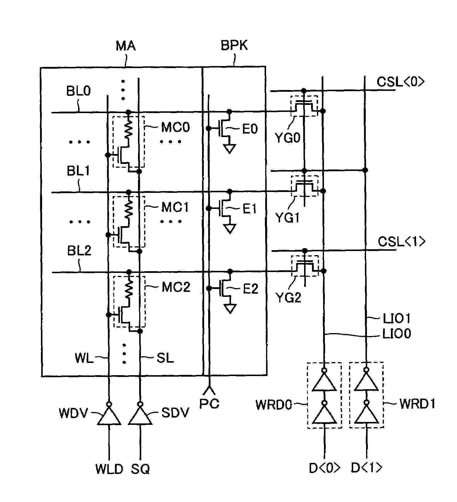
[0206]FIG. 20 schematically shows a construction of a main portion of the nonvolatile semiconductor memory device according to a second embodiment of the invention. The nonvolatile semiconductor memory device shown in FIG. 20 differs in the following points from the nonvolatile semiconductor memory device shown in FIG. 12. Specifically, in write drive circuit WRD, NAND gates NGA-NGD are further supplied with source line activating signal SLE. Source line drivers SDV are arranged on the opposite sides of each of source lines SL (SL00> and SL10>). Specifically, for memory array MA0, there are provided source line drivers SDV01 and SDV0u arranged on the opposite sides of source line SL00>, respectively, and for memory array MA1, there are provided source line drivers SDV11 and SDV1u arranged on the opposite sides of source line SL11>, respectively. Other constructions of the nonvolatile semiconductor memory device shown in FIG. 20 are the same as those of the nonvolatile semiconductor ...

third embodiment

[0240]FIG. 24 schematically shows a construction of a main portion of a nonvolatile semiconductor memory device according to a third embodiment of the invention. FIG. 24 shows a construction for writing and reading the data for one memory array MA.

[0241]The construction shown in FIG. 24 differs from the construction of the memory array shown in FIG. 4 in the following points. Source line drivers SDV0 and SDV1 are aligned to each other in a word line extending direction. Each source line is arranged corresponding to the bit lines in two columns equal in number to the bit width of write / read unit of the data. In FIG. 24, source lines SL0> and SL1> are arranged. Each of source lines SL0> and SL1> includes a main line portion MSL arranged parallel to bit line BL in the column direction (bit line extending direction), and feeder line portions SSL each arranged for the columns equal in number to the bit width of read / write data and parallel to word line WL and connected to main line porti...

fourth embodiment

[0251]FIG. 25 schematically shows a planar layout of the memory cells in the nonvolatile semiconductor memory device according to the fourth embodiment of the invention. In FIG. 25, active regions AR each for forming two memory cells are aligned in the row direction (word line extension direction) and the column direction (bit line extension direction). Each active region AR has a rectangular form elongated in the column direction, and is isolated by an isolation region (not shown) from others in the row and column directions.

[0252]Source lines SL1 and SL2 are arranged, in the row direction, crossing active regions AR. Source line contacts SCN electrically connect these source lines SL1 and SL2 to impurity regions in active regions AR, respectively. Word lines are arranged on both sides of each of source lines SL1 and SL2. Specifically, word lines WL0 and WL1 are arranged on both sides of source line SL1, respectively, and word lines WL2 and WL3 are arranged on both sides of source ...


PUM


Abstract

Source lines for a spin injection magnetic memory cell are arranged parallel to word lines for executing writing / reading of data multiple bits at a time. In a write operation, a source line potential changes in a predetermined sequence such that the source line commonly connected to a plurality of selected memory cells is set to pass a current only in one direction in each stage of the operation sequence. For the data write sequence, a current is caused to flow through memory cells according to write data sequentially, or the memory cell has a resistance state set to an initial resistance state before writing, and then changed to a state according to the write data Fast writing can be achieved in the magnetic memory without increasing a memory cell layout area.

Description

BACKGROUND OF THE INVENTION[0001]1. Field of the Invention[0002]The present invention relates to a nonvolatile semiconductor memory device, and particularly to a Magnetic Random Access Memory (MRAM) that nonvolatilely stores data, utilizing a magneto-resistance effect. More particularly, the present invention relates to a spin injection type MRAM which is configured to set magnetization directions, or the resistance state of a magnetic storage element by spin injection.[0003]2. Description of the Background Art[0004]The nonvolatile semiconductor memory device can hold storage data even when the power is shut down, and therefore it is not necessary to supply the power during a standby state. Therefore, the nonvolatile semiconductor memory devices have been widely used in portable equipments and others to which low power consumption is required.[0005]An MRAM utilizing a magneto-resistance effect is one of such nonvolatile semiconductor memory devices. In the MRAM, a storage element in...

Claims


Application Information

Patent Timeline
Patent Type & Authority Patents(United States)
IPC IPC(8): G11C11/00
CPCG11C11/16G11C11/5607G11C11/5685G11C13/0007G11C13/0069G11C2013/0078G11C2213/31G11C2213/79
Inventor TANIZAKI, HIROAKITSUJI, TAKAHARUMURAI, YASUMITSUHIDAKA, HIDETO
Owner RENESAS ELECTRONICS CORP
Why Eureka
Try Eureka