Method for process integration of non-volatile memory cell transistors with transistors of another type

a technology transistors, which is applied in the field of process integration of non-volatile memory cell transistors with transistors of another type, can solve the problems of increasing manufacturing time and expense, raising the level of contamination and defectivity of the semiconductor device, and forming sidewall spacers on the sides of the hv transistor gates that are not easily removed

Inactive Publication Date: 2008-10-21
NORTH STAR INNOVATIONS
View PDF32 Cites 45 Cited by
  • Summary
  • Abstract
  • Description
  • Claims
  • Application Information

AI Technical Summary

Problems solved by technology

However, in some semiconductor fabrication processes undesirable ONO sidewall spacers may be formed on the sides of the HV transistor gates that are not easily removed.
The presence of the ONO spacers may cause reliability issues with the HV transistors because charge traps in the nitride may cause unstable

Method used


Image

  • Method for process integration of non-volatile memory cell transistors with transistors of another type
  • Method for process integration of non-volatile memory cell transistors with transistors of another type
  • Method for process integration of non-volatile memory cell transistors with transistors of another type

Examples


Embodiment Construction

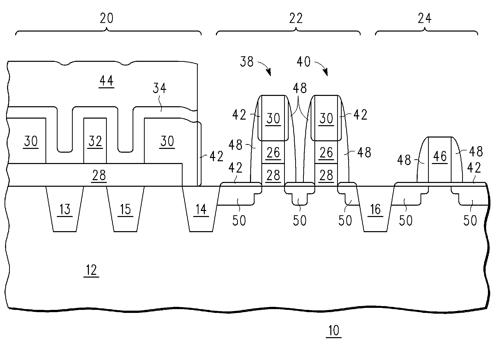
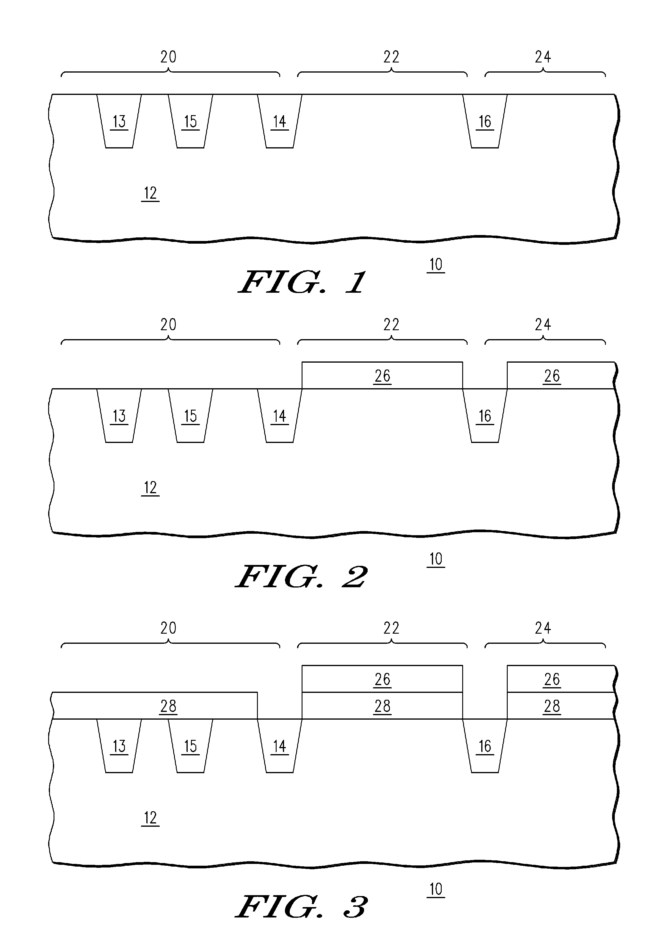
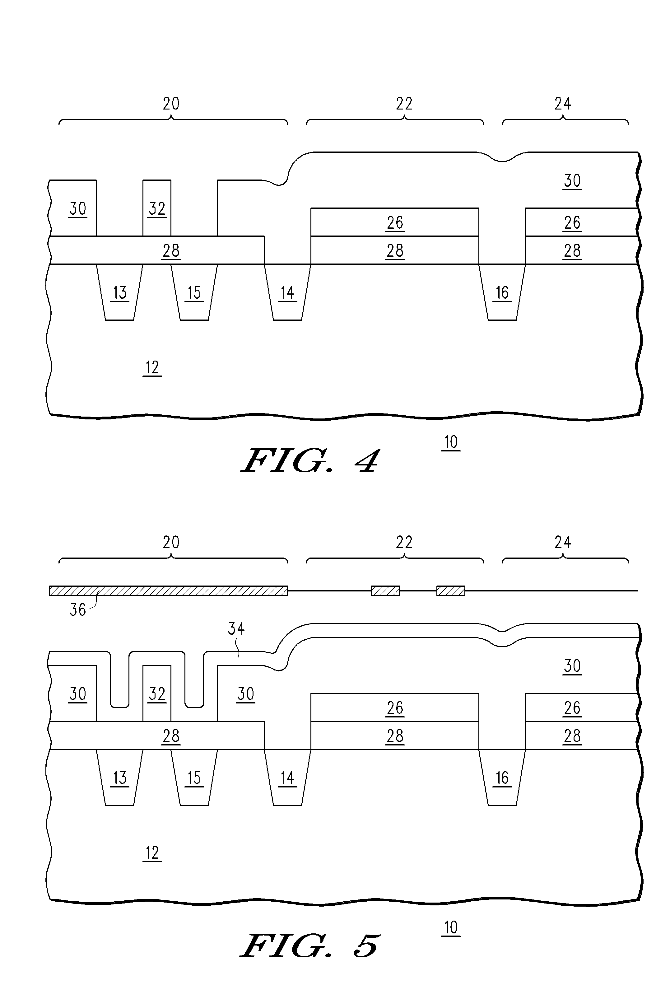
[0009]Generally, in one embodiment, the present invention provides a method for making a semiconductor device having non-volatile memory cell transistors, high voltage CMOS transistors, low voltage CMOS transistors, and having two polysilicon layers, where the non-volatile memory cell floating gates and the HV transistors are formed on a substrate using a first, or lower, polysilicon layer, and the LV transistors are formed using a second, or upper, polysilicon layer. The method includes forming a gate dielectric layer on the HV and LV regions. A tunnel oxide layer is formed under the substrate in the NVM region and over the gate dielectric in the HV and LV regions. A first polysilicon layer is formed over the tunnel dielectric layer and gate dielectric layer. The first polysilicon layer is patterned to form NVM floating gates. An ONO layer is formed over the first polysilicon layer. A single etch removal step is used to form one or more gates for the HV transistors from the first p...


PUM


Abstract

A method for making a semiconductor device having non-volatile memory cell transistors and transistors of another type is provided. In the method, a substrate is provided having an NVM region, a high voltage (HV) region, and a low voltage (LV) region. The method includes forming a gate dielectric layer on the HV and LV regions. A tunnel oxide layer is formed over the substrate in the NVM region and the gate dielectric in the HV and LV regions. A first polysilicon layer is formed over the tunnel dielectric layer and gate dielectric layer. The first polysilicon layer is patterned to form NVM floating gates. An ONO layer is formed over the first polysilicon layer. A single etch removal step is used to form gates for the HV transistors from the first polysilicon layer while removing the first polysilicon layer from the LV region.

Description

BACKGROUND[0001]1. Field[0002]This disclosure relates generally to semiconductor devices, and more specifically, to a method for process integration of non-volatile memory (NVM) cell transistors with transistors of another type.[0003]2. Related Art[0004]Many semiconductor devices include, or embed, non-volatile memory transistors with other transistor types on the same integrated circuit (IC). The manufacturing processes for the different transistor types may not be the same, requiring that the processes be integrated. For example, to integrate NVM with, for example, CMOS (complementary metal oxide semiconductor), the CMOS process may be modified to include the process steps necessary to fabricate the NVM memory cell and the supporting devices such as peripheral high voltage (HV) transistors and low voltage (LV) transistors.[0005]In most embedded NVMs, information is stored as charge on a “floating gate” which is completely surrounded by insulators, and which affects the threshold v...

Claims


Application Information

Patent Timeline
IPC IPC(8): H01L21/336
CPCH01L27/105H01L27/11526H01L27/11546H01L29/7833H10B41/40H10B41/49
Inventor PRINZ, ERWIN J.SHROFF, MEHUL D.
Owner NORTH STAR INNOVATIONS
Why Eureka
Try Eureka