Coil package and bias tee package

a technology of bias tee and coil, which is applied in the direction of transformer/inductance coil/winding/connection, multi-port network, radiating element structural forms, etc., can solve the problems of parasitic capacitance cannot be ignored, difficult to handle, and inability to use a coil, etc., to achieve enhanced frequency characteristics and easy handling

Inactive Publication Date: 2008-10-28
FUJITSU LTD
View PDF5 Cites 13 Cited by
  • Summary
  • Abstract
  • Description
  • Claims
  • Application Information

AI Technical Summary

Benefits of technology

[0026]The present invention has been made in view of the above points, and an object thereof is to provide a coil package which has a conical coil packaged therein without degrading the characteristics of the conical coil, thereby being made easy to handle, and being enhanced in frequency characteristics.
[0027]Another object of the present invention is to provide a bias tee package which has a conical coil and a capacitor packaged therein without degrading the characteristics of the conical coil, thereby being made easy to handle, and being enhanced in frequency characteristics.
[0029]To attain the other object, there is provided a bias tee package for supplying a high-frequency signal by superposing a DC component thereon. The bias tee package is characterized by comprising a cone / pyramid-shaped coil having a conical or pyramidal shape formed by a conductor wire wound around an outer peripheral surface of a core in a manner such that a winding diameter of the coil progressively decreases from one end to the other end of the coil, the cone / pyramid-shaped coil eliminating high-frequency components of the DC component, a capacitor for passing the high-frequency signal there through to eliminate low-frequency components, and a dielectric substrate, wherein the cone / pyramid-shaped coil, the capacitor, and the dielectric substrate are integrated with each other, by forming a hole in the dielectric substrate, for inserting a tip portion of the cone / pyramid-shaped coil, making a bottom of the hole and a back surface of the dielectric substrate electrically continuous by a first via, placing the cone / pyramid-shaped coil in the hole by directing a small-diameter side of the cone / pyramid-shaped coil toward the hole, electrically connecting the bottom of the hole and a tip-side lead wire extending from the cone / pyramid-shaped coil to each other, connecting an electrode on a large-diameter side of the cone / pyramid-shaped coil to an electrode on the dielectric substrate, cutting the dielectric substrate to form a cutout and disposing the capacitor in the cutout, and making opposite ends of the capacitor and the back surface of the dielectric substrate electrically continuous by a second via to thereby cause the tip-side lead wire and one end of the capacitor to be connected to each other.

Problems solved by technology

However, in performing optical communication at a transmission rate in the order of 40 Gb / s beyond the order of 10 Gb / s, it is impossible to use a coil of the above-mentioned type, since a parasitic capacitance of the coil itself and earth capacitances thereof cannot be ignored and a self-resonance frequency thereof forms a stumbling block to the use in such an optical communication.
However, when the coil 100 is used as a high-frequency circuit, the parasitic capacitance cannot be ignored.
Therefore, it can be used in limited areas or locations of devices, and is very difficult to handle.
Moreover, the characteristics of the conical coil 110 vary with the mounting angle thereof, and hence there is a problem that a large variation in the characteristics is caused when the conical coil 110 is mounted.
Therefore, the conical coils 110 are mounted on circuit boards one by one, by bonding, which makes it impossible to expect improvement of productivity.

Method used


Image

  • Coil package and bias tee package
  • Coil package and bias tee package
  • Coil package and bias tee package

Examples


Embodiment Construction

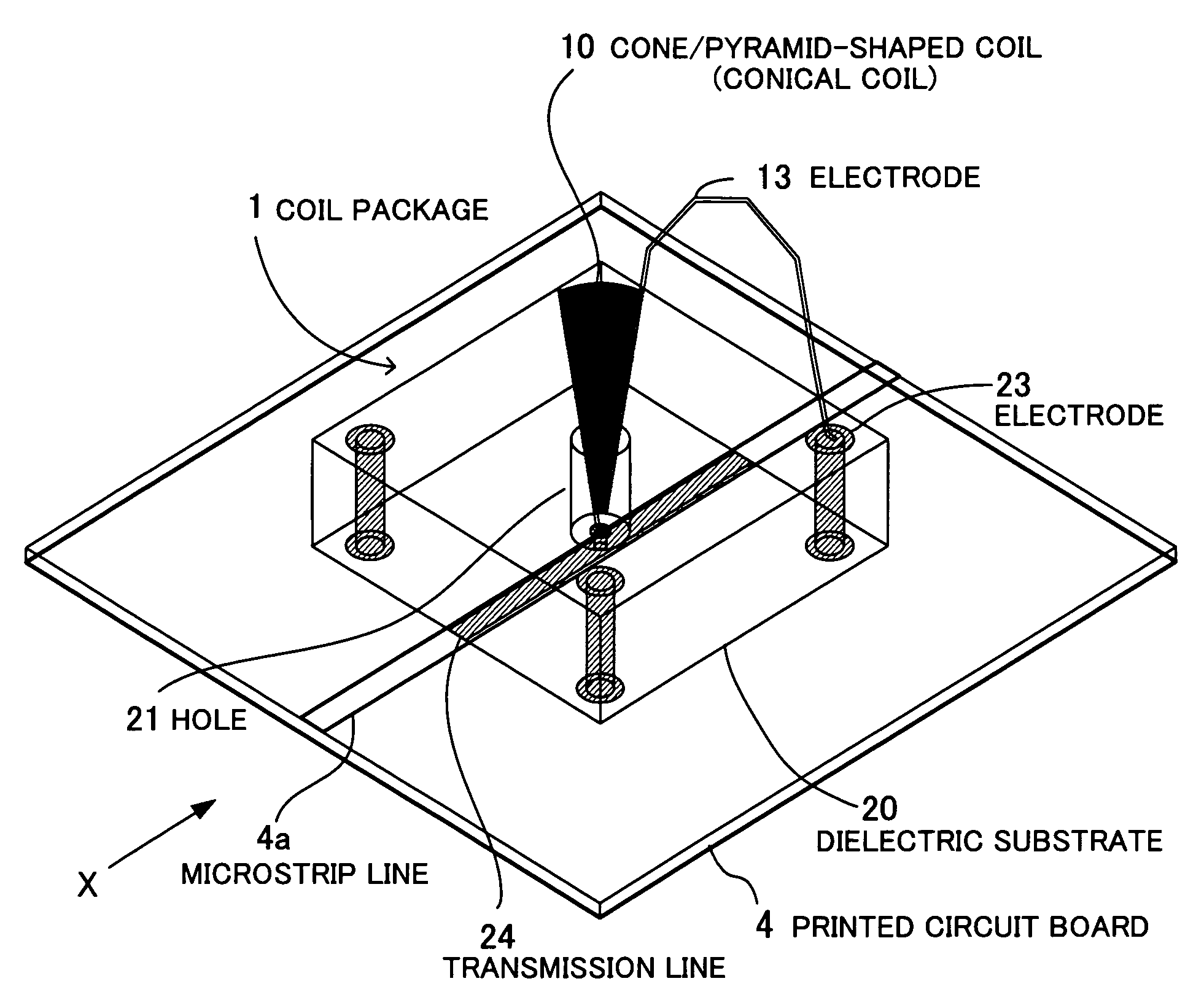
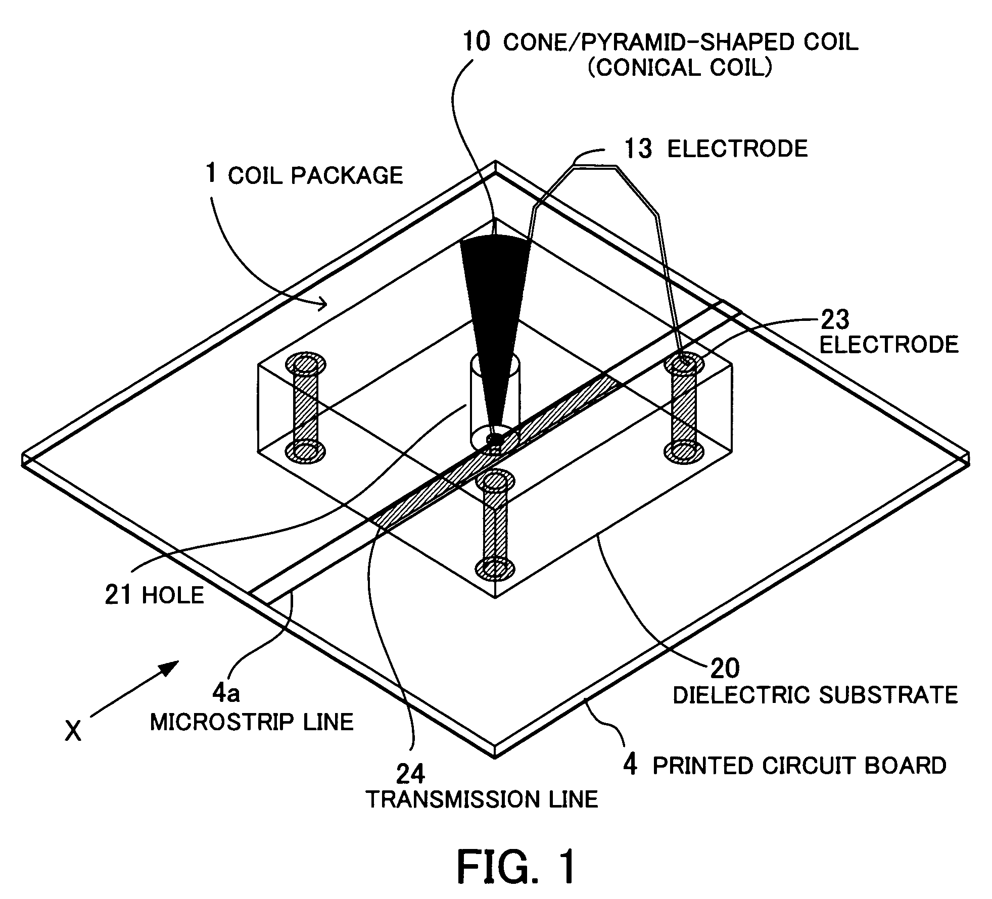
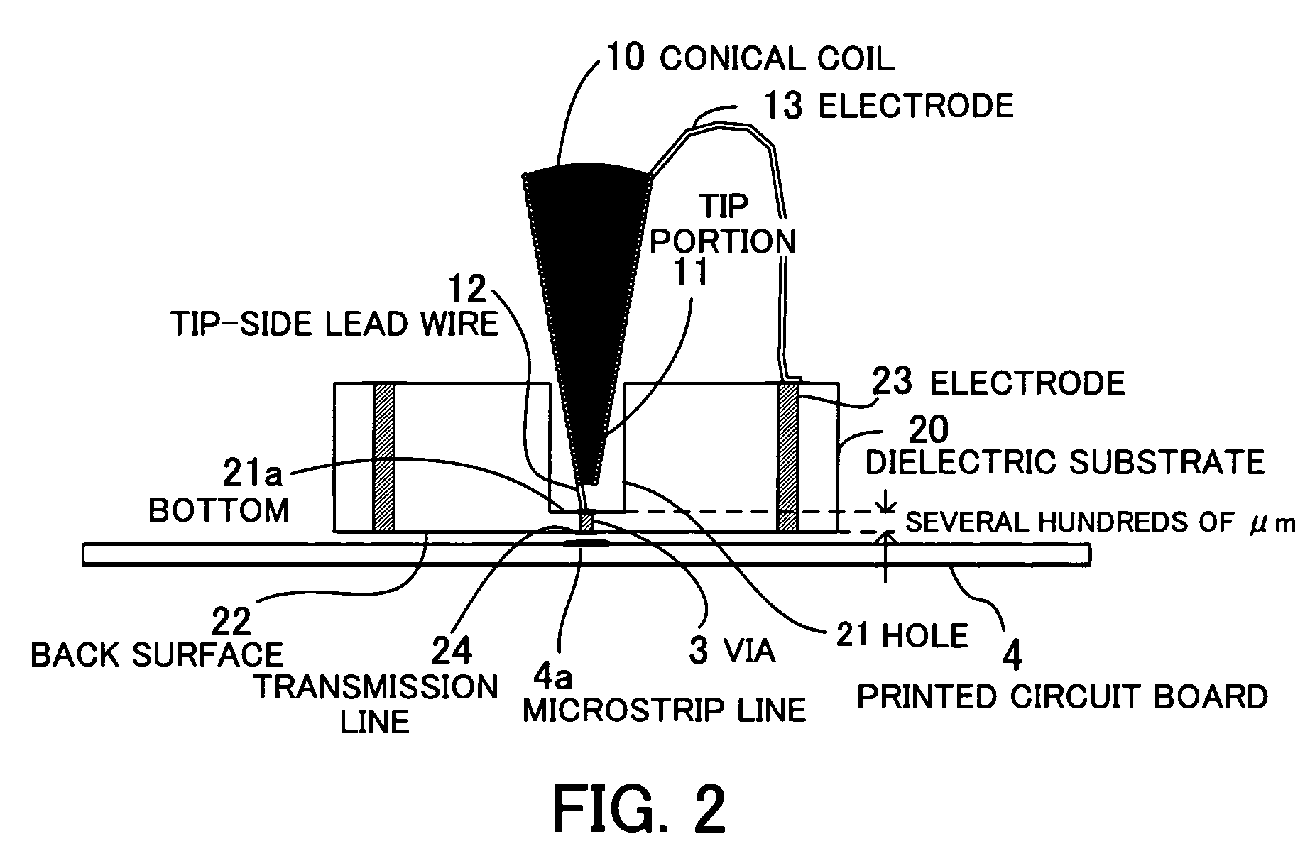
[0051]The present invention will now be described in detail with reference to the accompanying drawings showing preferred embodiments thereof. FIGS. 1 and 2 are a schematic perspective view and a schematic side view of a coil package according to a first embodiment of the present invention, in which FIG. 2 shows the coil package as viewed from the X direction in FIG. 1. The coil package 1 according to the first embodiment is comprised of a dielectric substrate 20, and a cone / pyramid-shaped coil 10. The cone / pyramid-shaped coil 10 is a coil having a conical or pyramidal shape formed by a conductor wire wound around an outer peripheral surface of a core in a manner such that the winding diameter of the conductor wire progressively decreases from one end to the other end of the coil, as described hereinbefore with reference to FIG. 18. Hereinafter, the cone / pyramid-shaped coil 10 is referred to as “the conical coil 10”.

[0052]As shown in FIGS. 1 and 2, the dielectric substrate 20 made o...


PUM

PropertyMeasurementUnit
sizeaaaaaaaaaa
impedanceaaaaaaaaaa
thicknessaaaaaaaaaa

Abstract

A coil package which makes it easy to handle a high-frequency cone / pyramid-shaped coil and enhance frequency characteristics without degrading the characteristics of the coil. The cone / pyramid-shaped coil has a conical or pyramidal shape formed by wiring a conductor wire around an outer peripheral surface of a core such that the winding diameter of the coil progressively decreases from one end to the other end of the coil. The coil and a dielectric substrate are integrated with each other by forming a hole for inserting a tip portion of the coil in the dielectric substrate, making the bottom of the hole and a back surface of the dielectric substrate electrically continuous by a via, placing the coil in the hole by directing a small-diameter side of the cone / pyramid-shaped coil to the hole, electrically connecting the bottom of the hole and a tip-side lead wire extending from the coil to each other, and connecting an electrode on a large-diameter side of the coil to an electrode on the dielectric substrate.

Description

CROSS-REFERENCE TO RELATED APPLICATIONS[0001]This application is based upon and claims the benefits of priority from the prior Japanese Patent Application No. 2005-298347, filed on Oct. 13, 2005, the entire contents of which are incorporated herein by reference.BACKGROUND OF THE INVENTION[0002]1. Field of the Invention[0003]This invention relates to a coil package and a bias tee package, and more particularly to a coil package having a high-frequency coil mounted therein, and a broadband bias tee package for supplying a high-frequency signal by superposing a DC component on the high-frequency signal.[0004]2. Description of the Related Art[0005]Recently, with the development of multi-media technology, there is an increasing demand for constructing optical communication networks that transmit high-speed, large-volume information at low costs over long distances. To meet the demand, there have been developed optical communication systems whose transmission rate is in the order of 10 Gb...

Claims


Application Information

Patent Timeline
Patent Type & Authority Patents(United States)
IPC IPC(8): H01F27/28H03H7/00
CPCH01F5/00H01Q1/36H01Q19/09H01F27/027H01F2005/006H05K1/0243
Inventor YAGISAWA, TAKATOSHIIKEUCHI, TADASHIKURODA, YASUHIDECHEUNG, TSZSHING
Owner FUJITSU LTD
Why Eureka
Try Eureka