Non-contact electrical connections test device

a test device and non-contact technology, applied in electrical testing, electrical testing, electronic circuit testing, etc., can solve the problems of difficult electrical testing and inability to be done by peopl

Inactive Publication Date: 2008-11-04
COMMISSARIAT A LENERGIE ATOMIQUE ET AUX ENERGIES ALTERNATIVES
View PDF6 Cites 0 Cited by
  • Summary
  • Abstract
  • Description
  • Claims
  • Application Information

AI Technical Summary

Benefits of technology

[0010]Alternatively, for a test involving both a conductor of the front face and a conductor of the rear face of the substrate to be tested, it is possible to provide for charging a conductor without contact on the side where the conductors are more dense and to apply a potential by direct contact on the side where the conductors, less dense, are more easily accessible.
[0021]By the superimposition of two open-work grids forming both the collector electrode and the measuring capacitor associated with it, the transparency of the collector plate with respect to the illuminating beam is maximized without reducing the capacity value of the capacitor too much.

Problems solved by technology

With the reduction of the dimensions of integrated circuits and the increase in the density of the connections, electrical testing becomes difficult and can no longer be done by direct contact between test points and the conductive areas to be tested.

Method used


Image

  • Non-contact electrical connections test device
  • Non-contact electrical connections test device
  • Non-contact electrical connections test device

Examples


Embodiment Construction

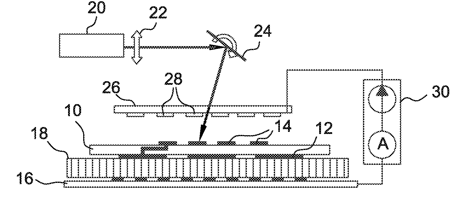
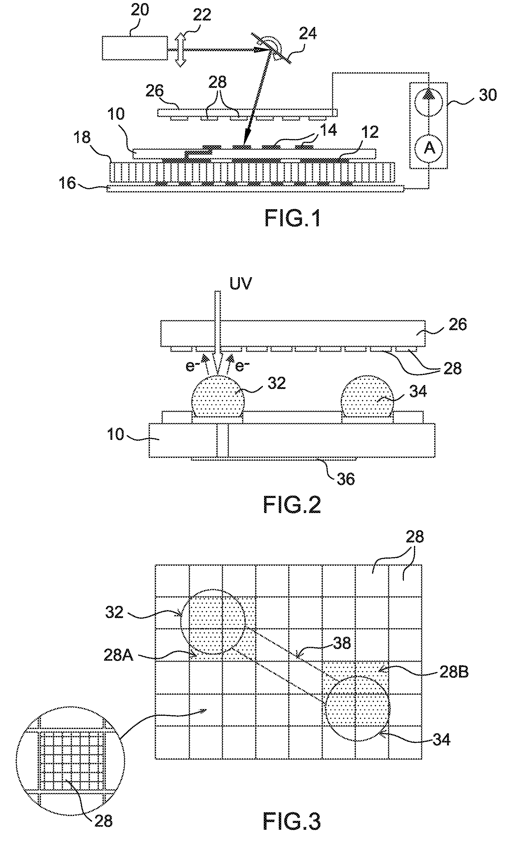
[0030]The general principle of a non-contact test is shown diagrammatically in FIG. 1. The substrate to be tested is given the reference 10; it is for example of the type known as a “chip carrier” having multiple interconnections between a rear face (at the bottom of the figure) and a front face (at the top of the figure). The rear face is intended to be soldered on a printed circuit and the front face is intended to receive an integrated circuit chip. The connections of the rear face are given the reference 12. They principally comprise soldering areas making it possible to solder the substrate directly onto a printed circuit. The connections of the front face, more dense than those of the rear face, are given the reference 14. These connections 14 principally comprise contact pads, or soldering areas, making it possible to connect, by direct soldering, that area directly to an output pin of a printed circuit chip (soldering of the “flip-chip” type, that is to say with the chip tur...


PUM


Abstract

A non-contact testing of electrical characteristics of substrates carrying dense electrical connections is non-contact in that an injection or an extraction of electrons in the conductors to be tested, is obtained by an electron tearing effect under the effect of an electromagnetic beam of ultraviolet rays. The test device has an electron collector plate conformed as an array of individually addressable electrodes, able to be taken to a positive or negative potential in order to carry out an injection or an extraction of electrons. A capacitor is associated with each electrode. The individual electrode is produced in the form of an open-work conductive grid constituting a first plate of the capacitor. The other plate is constituted by an open-work grid situated plumb with the first one.

Description

RELATED APPLICATIONS[0001]The present application is based on, and claims priority from, France Application Number 06 01385, filed Feb. 17, 2006, the disclosure of which is hereby incorporated by reference herein in its entirety.BACKGROUND OF THE INVENTION[0002]1. Field of the Invention[0003]The invention relates to the non-contact testing of electrical characteristics of electronic components, such as the insulation between conductors, the electrical continuity of conductors, resistance, and even capacity and inductance. The testing is non-contact in the sense that an injection or an extraction of electrons in the conductors to be tested is obtained by an electron tearing effect under the effect of an electromagnetic beam (in principle a beam of ultraviolet rays) having a photon energy greater than the energy for extracting an electron from the conductor.[0004]2. Brief Description of the Related Art[0005]Non-contact test devices are principally intended for checking the electrical ...

Claims


Application Information

Patent Timeline
Patent Type & Authority Patents(United States)
IPC IPC(8): G01R31/302
CPCG01R31/305
Inventor DEMARS, PATRICK
Owner COMMISSARIAT A LENERGIE ATOMIQUE ET AUX ENERGIES ALTERNATIVES
Why Eureka
Try Eureka