
Method of manufacturing flash memory device

a technology of flash memory and manufacturing method, which is applied in the direction of semiconductor devices, basic electric elements, electrical equipment, etc., can solve the problems of several limits in the flash memory cell, and achieve the effects of improving programming speed, increasing phosphorus concentration, and reducing coupling ratio

Inactive Publication Date: 2008-11-11
SK HYNIX INC
View PDF9 Cites 1 Cited by
  • Summary
  • Abstract
  • Description
  • Claims
  • Application Information

AI Technical Summary

Benefits of technology

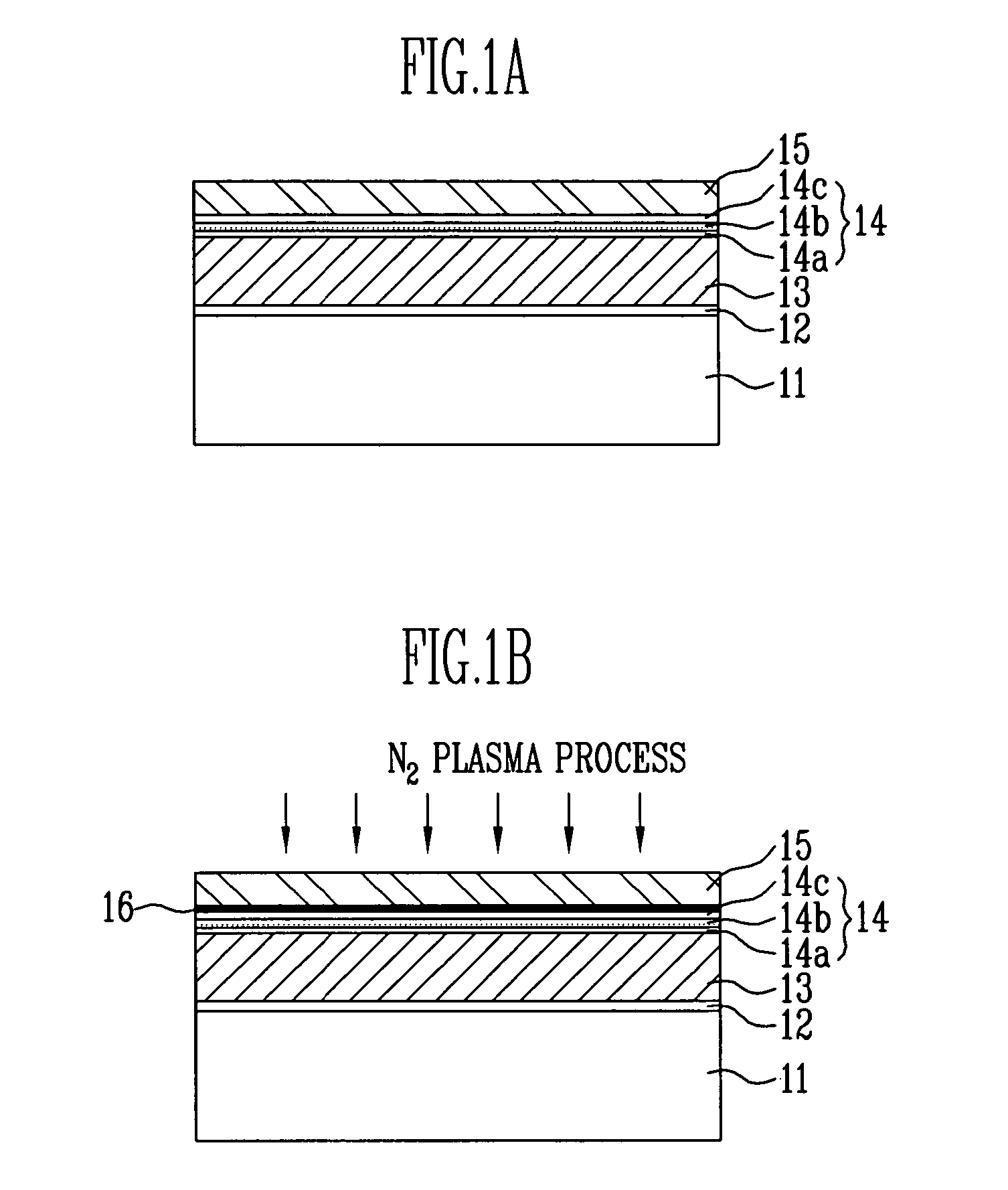
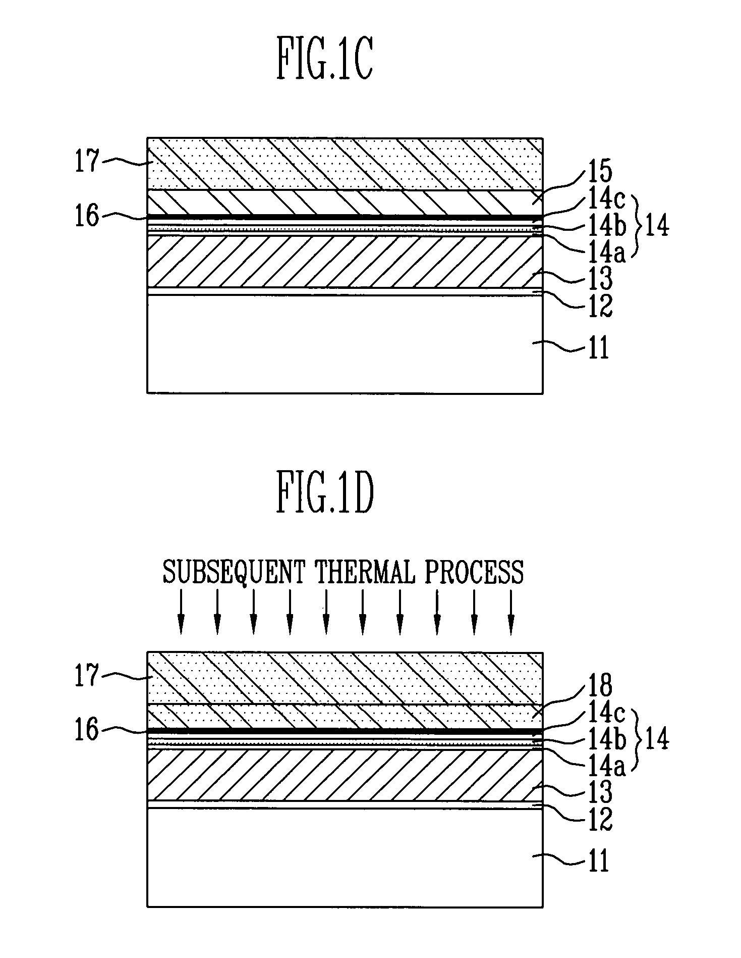
The present invention provides a method of manufacturing a flash memory device that improves programming speed by increasing the phosphorus concentration of the polysilicon layer used as a control gate, without reducing the coupling ratio. This is achieved by forming an undoped polysilicon layer over a semiconductor substrate where a floating gate and a dielectric layer are formed, and then applying N2 plasma to the undoped polysilicon layer to form a heavily doped polysilicon layer. A nitrogen layer is formed at the interfaces between the dielectric layer and the undoped polysilicon layer during the N2 plasma process. During a re-oxidization process, it is possible to prevent the thickness of the dielectric layer from being increased by reducing diffusion speed, phosphorous, and oxygen. Additionally, phosphorous of the heavily-doped polysilicon layer is diffused into the undoped polysilicon layer in a subsequent process, thereby increasing the phosphorous concentration of the undoped polysilicon layer. This results in improved programming speed by increasing the doping concentration of the control gate without a variation of the coupling ratio.

Problems solved by technology

However, there are several limits in the flash memory cell in conditions of low voltage.

Method used


Image

  • Method of manufacturing flash memory device
  • Method of manufacturing flash memory device
  • Method of manufacturing flash memory device

Examples


Embodiment Construction

[0014]The present invention will be described below in more detail using specific embodiment and the accompanying drawings. The present invention may, however, be embodied in different forms and should not be constructed as limited to the embodiments set forth herein. Like numerals refer to like elements throughout the specification.

[0015]It will be understood that, although the terms first, second, etc. may be used herein to describe various elements, these elements should not be limited by these terms. These terms are only used to distinguish one element from another. For example, a first element could be termed a second element, and, similarly, a second element could be termed a first element, without departing from the scope of the present invention. As used herein, the term “and / or” includes any and all combinations of one or more of the associated listed items.

[0016]It will be understood that when an element such as a layer, region, or substrate is referred to as being “on” or...


PUM


Abstract

Provided is a method of manufacturing a flash memory device. In accordance with the present invention, an undoped polysilicon layer is formed over a semiconductor substrate where a floating gate and a dielectric layer are formed. By performing N2 plasma process with respect to the undoped polysilicon layer, a heavily doped polysilicon layer is formed to form a control gate. Due to N2 plasma process, a nitrogen layer is formed at the interfaces between the dielectric layer and the undoped polysilicon layer. As a result, during a re-oxidization process, it is possible to prevent a thickness of the dielectric layer from being increased by reducing diffusion speed phosphorous and oxygen. Additionally, phosphorous of the heavily doped polysilicon layer is diffused into the undoped polysilicon layer in a subsequent process, thereby increasing a phosphorous concentration of the undoped polysilicon layer. Accordingly, it is possible to improve a program speed by increasing a doping concentration of the control gate without a variation of coupling ratio.

Description

BACKGROUND OF THE INVENTION[0001]The present invention relates to methods of manufacturing flash memory devices, and more particularly to a method of manufacturing a flash memory device capable of improving programming speed by increasing the phosphorous concentration of the polysilicon layer used as the control gate, but not reducing coupling ratio.[0002]In general, a typical flash memory cell is embodied by forming a gate and source / drain. The gate is comprised of a sequentially stacked structure of tunnel oxide, a floating gate, a dielectric layer, and a control gate at predetermined regions over a semiconductor substrate. The source / drain is formed at both sides of the gate on the semiconductor substrate. Such a flash memory cell is programmed or erased by injecting or emitting electrons to the floating gate, thereby generating hot carriers through a lateral surface of the drain. In addition, the program operation is performed by injecting hot carriers into the floating gate thr...

Claims


Application Information

Patent Timeline
Patent Type & Authority Patents(United States)
IPC IPC(8): H01L21/225H10B69/00
CPCH01L21/28273H01L29/40114H10B43/30H10B43/40
Inventor CHOI, SE KYOUNG
Owner SK HYNIX INC
Learn More