Display device

a display device and display technology, applied in the field of display devices, can solve the problems of adversely increasing power consumption, unable to ensure sufficient aperture rate, and unable to obtain the required display luminance, and achieve the effect of simplifying configuration and manner

Inactive Publication Date: 2008-11-11
JAPAN DISPLAY CENT INC
View PDF5 Cites 69 Cited by
  • Summary
  • Abstract
  • Description
  • Claims
  • Application Information

AI Technical Summary

Benefits of technology

[0011]An object of the present invention to provide a display device capable of performing image pro

Problems solved by technology

At this time, if a lot of photoelectric conversion elements and circuits are integrated in the pixels, it is impossible to ensure sufficient aperture rate, and to obtain required display luminance.
The luminance of the backlight may be able to raise by some way, but this may, in turn, adversely i

Method used


Image

  • Display device
  • Display device
  • Display device

Examples


embodiment 2

[0135]A second embodiment of the present invention also relies upon the feature called field sequential drive where the backlight has a set of luminescent colors lit up in a repetitive sequence of red, green and blue. In such a case, an observer visually perceives as if multi-color images were displayed.

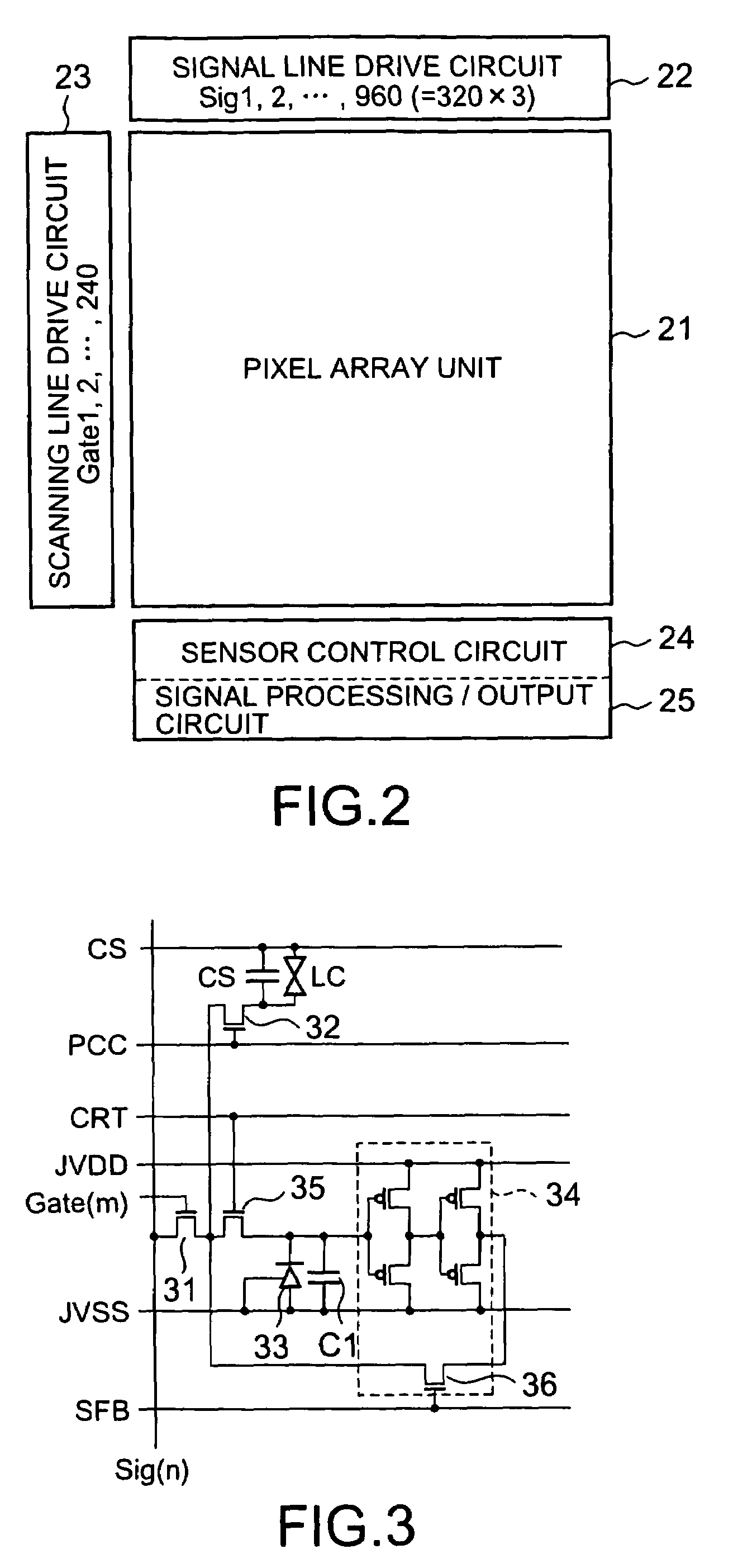
[0136]A structure of a single pixel unit in the second embodiment is similar to that in FIG. 3. As shown in FIG. 3, the single pixel includes merely a single image acquisition sensor 33, thereby attaining a sufficient aperture rate. Thus, as will be recognized from the layout in FIG. 25, each pixel leaves a sufficient vacant area surrounding a patch of the image acquisition sensor 33, and the image acquisition sensor 33 may be omnidirectionally displaced within a confinement of the single pixel.

[0137]In view of this noteworthy point, as shown in FIG. 26, according to the present embodiment, the image acquisition sensors 33 in the pixels may be deployed in a zigzag formation along the...

embodiment 3

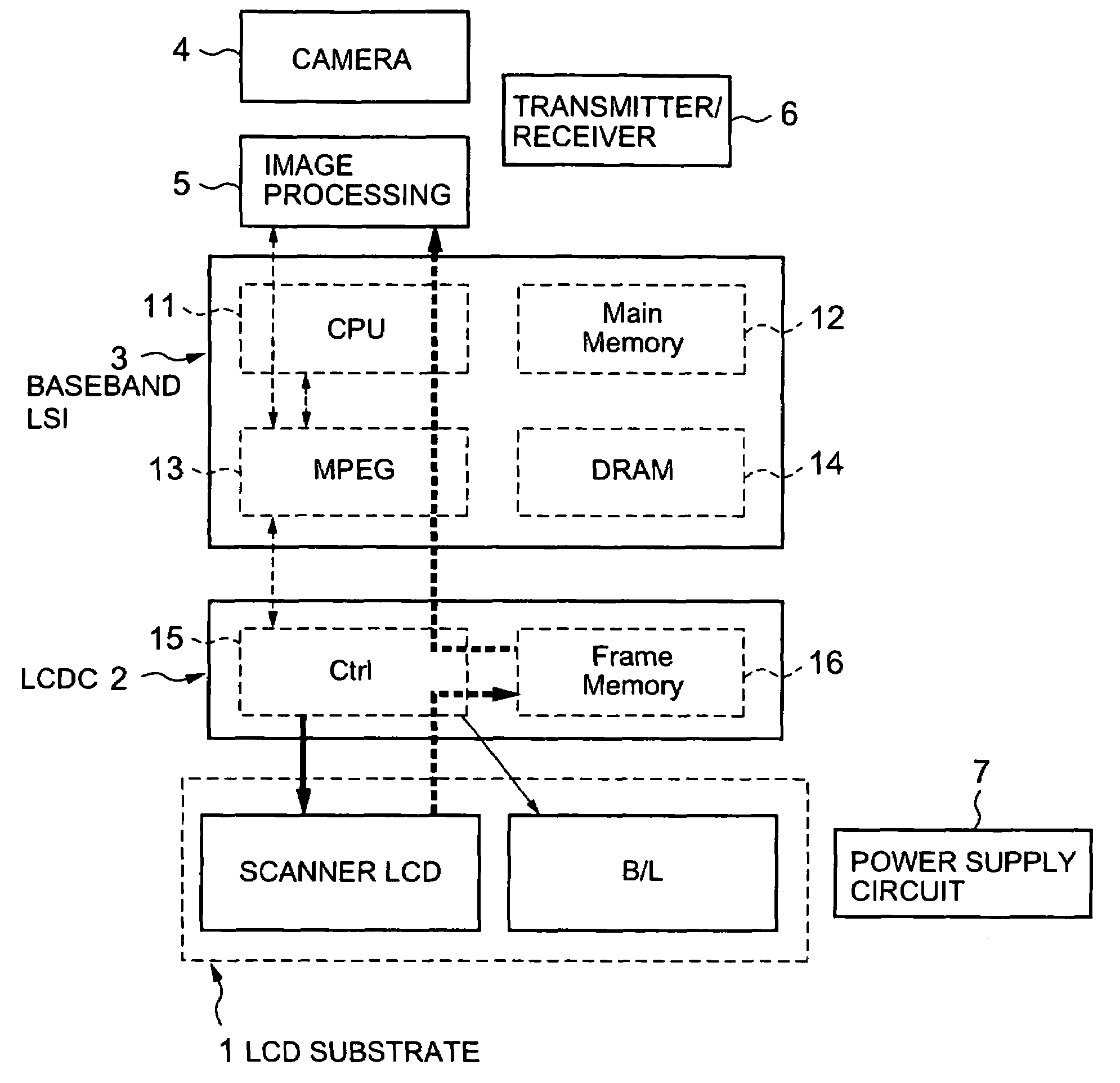
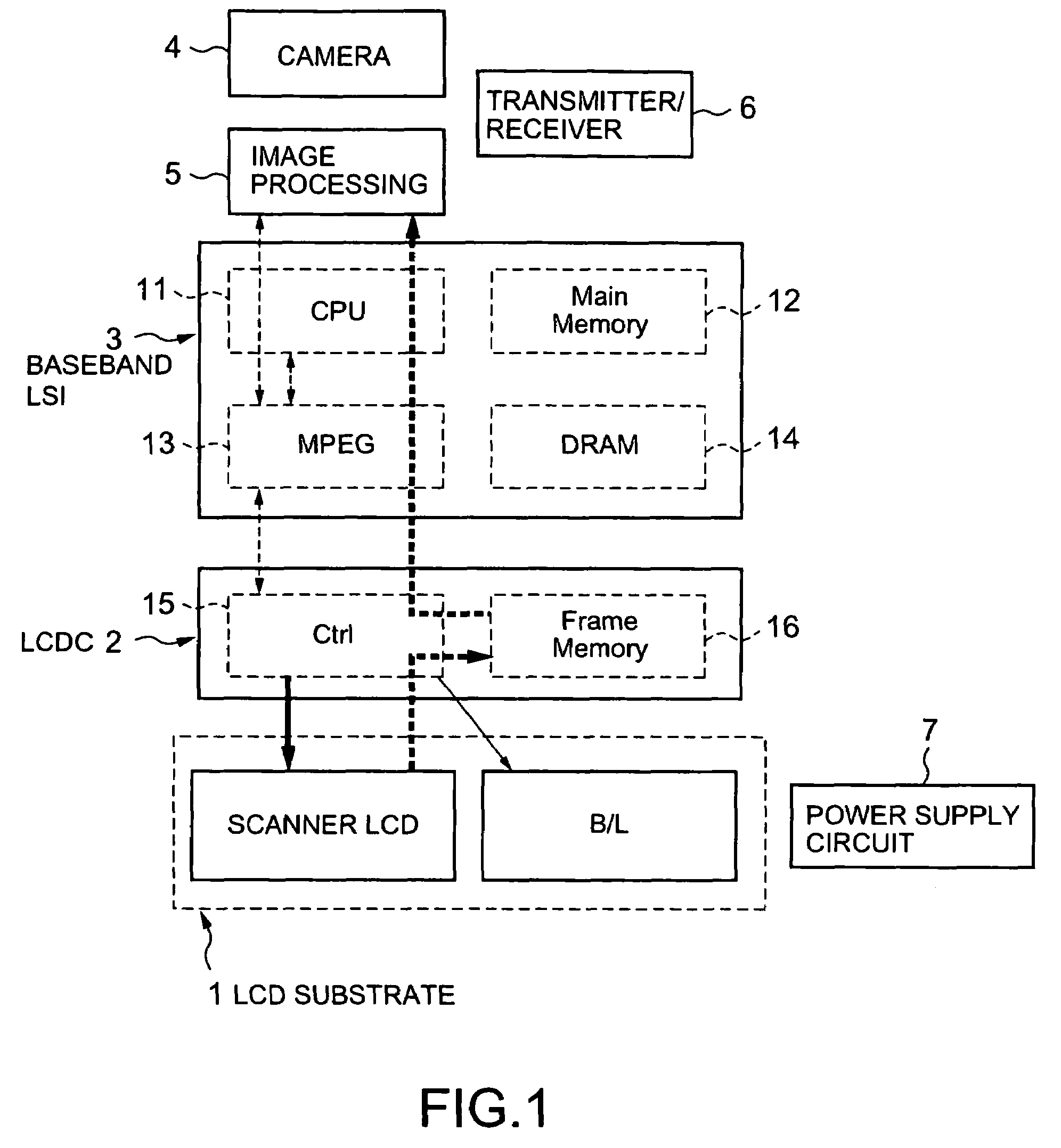
[0143]A third embodiment of the present invention relates to system configuration. FIG. 29 is a conventional block diagram. No signal is transmitted from the LCDC 2 to the CPU 11, or from the LCDC 2 to the image processing IC 5 of the camera 4. The image processing IC 5 conducts a prescribed image processing for the image pickup by the camera 4. The image data is transmitted to the CPU 11 in a prescribed format such as Yuv format. The CPU 11 transmits the image data to the LCDC 2 at a prescribed timing. The LCDC 2 transmits the digital image data to the LCDC at a prescribed timing, for example, by accumulating the image data transmitted from the CPU 11 to the frame memory. The LCDC conducts display operation based on the digital image data.

[0144]FIG. 30 is a diagram showing system configuration according to this embodiment. One feature of FIG. 30 is to have a bidirectional interface between the LCDC 2 and the CPU 11. The image pickup data is once stored in the memory of the LCDC 2, ...

embodiment 4

[0145]A fourth embodiment of the present invention relates to system configuration. FIG. 31 is a diagram showing system configuration according to this embodiment. One feature of FIG. 31 is to have a dedicated interface between the LCDC 2 and the image processing IC 5. The image pickup data is once stored in the memory of the LCDC 2, and directly transmitted to the image processing IC 5 based on “request from the image processing IC 51” or “instruction from the CPU 11”, to conduct general image processing. When the image pickup data is transmitted to the image processing IC 5, the CPU bus is not occupied. Accordingly, large load is not imposed on the CPU 11. Since configurations of the LCDC 2, the image processing IC 5 and the LCD 1 are the same as those of the first, second and third embodiments, the explanation will be omitted.


PUM


Abstract

A display device, comprising: a pixel array unit having display elements formed in vicinity of intersections of signal lines and scanning lines arranged in length and breadth, image pickup units and an output unit which outputs binary data corresponding to image picked up by said image pickup unit; a image pickup device provided separate from said image pickup unit; a first image processing unit configured to generate multiple gradation data based on multiple binary data picked up by said image pickup units based on multiple image pickup conditions; and a second image processing unit configured to receive either the image pickup data picked up by said image pickup device or the multiple gradation data generated by said first image processing unit, to conduct a prescribed image processing.

Description

CROSS REFERENCE TO RELATED APPLICATIONS[0001]This application claims benefit of priority under 35 USC § 119 to Japanese Patent Applications No. 2003-96373, No. 2003-96432 and No. 2003-96519, filed on Mar. 31, 2003, the entire contents of which are incorporated by reference herein.BACKGROUND OF THE INVENTION[0002]1. Field of the Invention[0003]The present invention relates to a display device having an image acquisition function.[0004]2. Related Background Art[0005]A liquid crystal display is typically comprised of an array substrate having signal lines, scanning lines and pixel TFTs arranged in matrix, and a drive circuit for driving the signal lines and the scanning lines. With an integrated circuit technology drastically advanced in recent years, a processing technology forming a part of the driving circuits on the array substrate has been put into practical use. Thanks to the technology, it became possible to downsize and lighten the entire liquid crystal display. Such kind of li...

Claims


Application Information

Patent Timeline
IPC IPC(8): G09G3/36G06K9/00
CPCG09G3/3648G09G2300/0842G09G2300/0876G09G2300/088B24C5/02B24C7/0046
Inventor NAKAMURA, TAKASHIHAYASHI, HIROTAKA
Owner JAPAN DISPLAY CENT INC
Why Eureka
Try Eureka