Integrated laser-diffractive lens device

a laser-diffractive lens and integrated technology, applied in semiconductor lasers, laser cooling arrangements, laser details, etc., can solve the problems of difficult fabrication of devices and sensitive optical characteristics to wafer thickness errors, and achieve the effect of facilitating economical manufacturing and minimizing the number of individual parts and structural elements

Inactive Publication Date: 2008-11-11
BROADCOM INT PTE LTD
View PDF5 Cites 14 Cited by
  • Summary
  • Abstract
  • Description
  • Claims
  • Application Information

AI Technical Summary

Benefits of technology

[0010]The device can be coupled directly to an optical fiber without using a separate lens because the beam emerges from the device already focalized or collimated. (Nevertheless, a lens, such as an economical ball lens, can be used if desired.) Furthermore, the above-described surface-emitting arrangement facilitates economical manufacture because not only does the structure minimize the number of individual parts and structural elements, but also the anti-reflective coating (i.e., a coating of the type that is commonly applied to the laser emission facet at the chip edge of a conventional device) can be applied to the entire wafer upper surface before dicing the wafer into individual chips. Also, the surface-emitting arrangement of the devices enables them to be tested before dicing the wafer into individual chips by applying probes to electrical contacts formed in the chip surface and measuring radiation emitted from the chip surface in response.

Problems solved by technology

Nevertheless, the device is not straightforward to fabricate due to the inclusion of a waveguide to direct the beam from the laser toward the angled surface.
Also, the geometry of the device may make its optical characteristics sensitive to wafer thickness errors.

Method used


Image

  • Integrated laser-diffractive lens device
  • Integrated laser-diffractive lens device
  • Integrated laser-diffractive lens device

Examples


Embodiment Construction

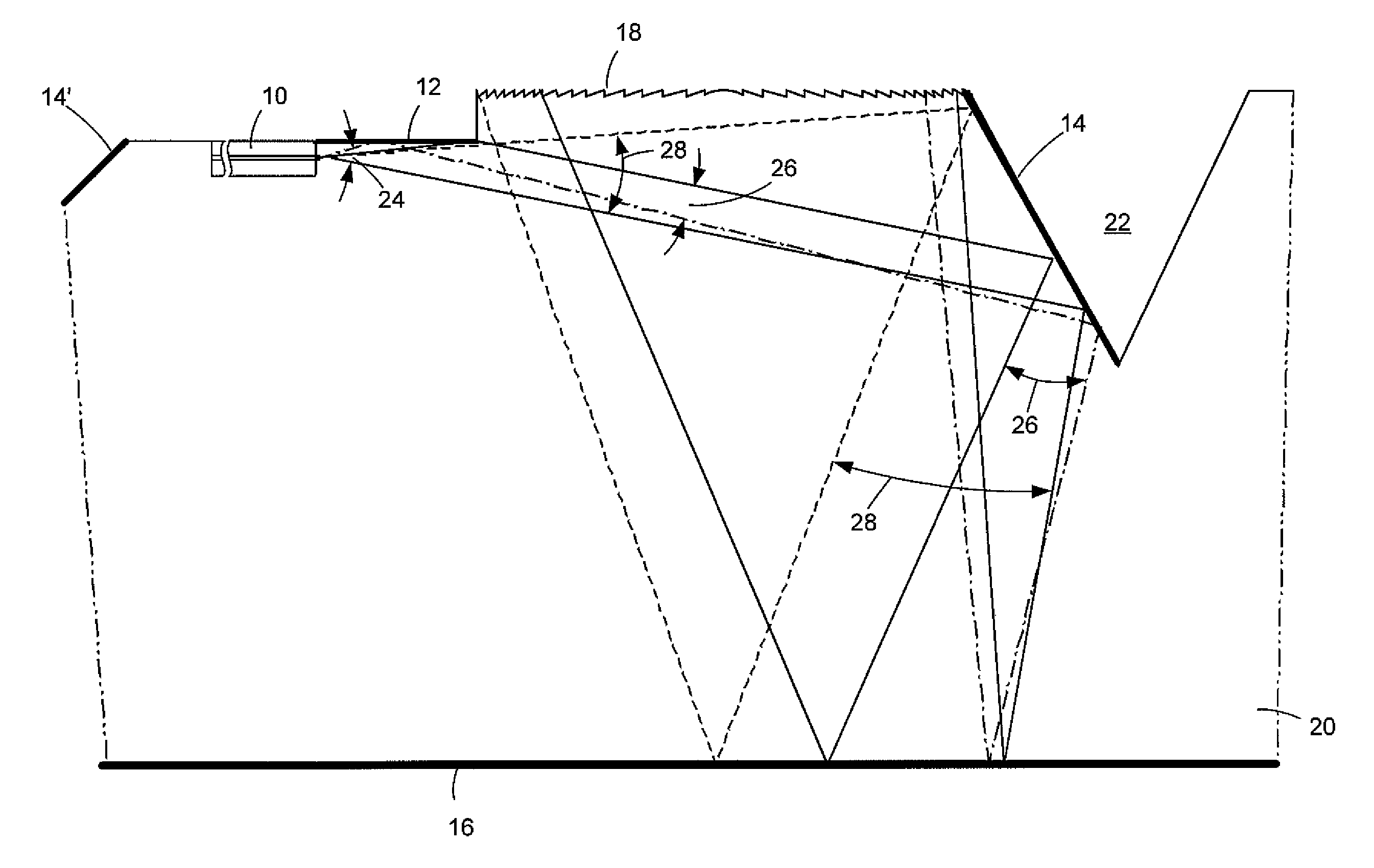
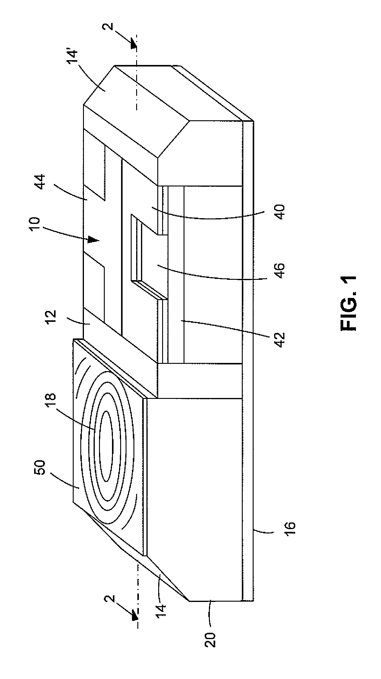
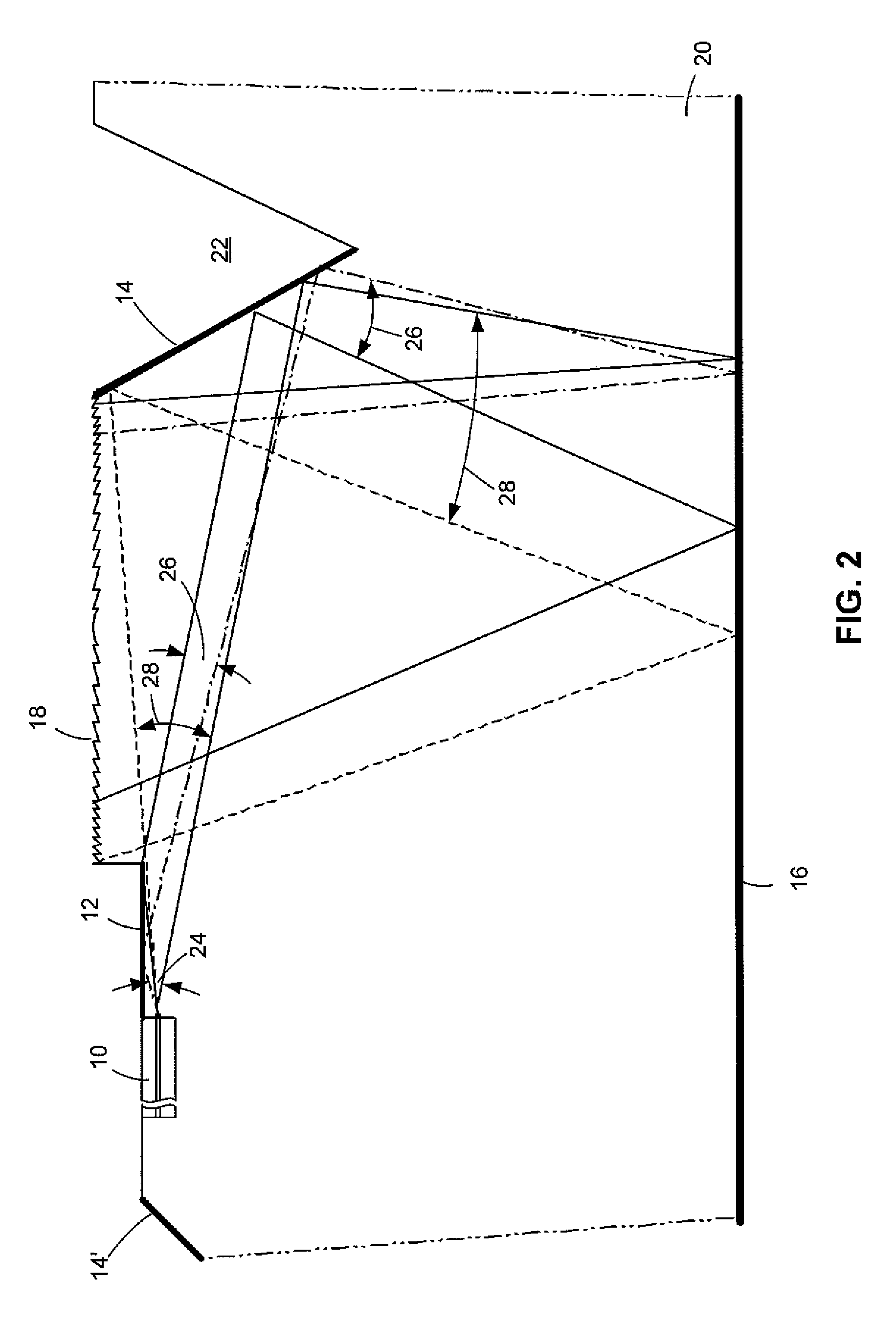
[0015]As shown in FIG. 1 (not to scale), in an illustrative or exemplary embodiment of the invention, a laser device includes an edge-emitting laser 10, an upper mirror 12, an angled mirror 14, a lower mirror 16, and a diffractive lens 18. These elements are formed on or in a suitable semiconductor substrate 20, such as doped indium phosphide (InP). The formation of such lasers is well known in the art but is nonetheless described in some additional detail below. Note that the term “mirror” is used herein for purposes of convenience and clarity and in accordance with its ordinary meaning in the art to refer to a surface that is highly or substantially reflective with respect to the radiation wavelengths emitted by laser 10. The reflection on upper mirror 12 is obtained by total reflection.

[0016]As shown in FIG. 2 (not to scale), substrate 20 has a generally planar or flat, bar-like shape, in accordance with conventional chip technologies in which a large number of devices (chips) ar...


PUM


Abstract

A semiconductor laser device includes an edge-emitting laser monolithically integrated with a diffractive lens formed on the chip surface to emit a focalized or collimated beam in a direction perpendicular to the surface. An upper reflective surface and an angled reflective surface are formed in the chip upper surface. A lower reflective surface is formed in the chip lower surface. The laser, angled reflective surface, upper reflective surface, lower reflective surface and diffractive lens are oriented in relation to one another so that a first portion of the light emitted by the laser impinges directly upon the upper reflective surface, which reflects it onto the angled reflective surface, while a second portion of the light emitted by the laser impinges directly upon the angled reflective surface. The angled reflective surface reflects the light portions onto the lower reflective surface, which in turn reflects them through the diffractive lens.

Description

TECHNICAL FIELD OF THE INVENTION[0001]The invention relates generally to semiconductor lasers and, more specifically, to a device in which a laser and diffractive lens are integrated with each other on the same chip.BACKGROUND OF THE INVENTION[0002]Semiconductor lasers are commonly used in optical transceivers for telecommunications and data communication networks. The lasers used in such optical transceivers are commonly of the edge-emitting type. The edge-emitting laser of an optical transceiver is commonly coupled to the fiber with an aspheric lens or other discrete optical element because the light that the laser emits is not focalized or collimated, i.e., it diverges in a cone shape as it propagates. While the use of lenses to couple edge-emitting lasers to fibers in optical transceivers works reasonably well, it would be desirable to improve transceiver manufacturing economy by minimizing the number of transceiver parts and the attendant steps needed to achieve optical alignme...

Claims


Application Information

Patent Timeline
Patent Type & Authority Patents(United States)
IPC IPC(8): H01S5/00
CPCH01S5/0267H01S5/0071H01S5/0207H01S5/026
Inventor TALLONE, LUIGIROGGERO, GUIDO ALBERTO
Owner BROADCOM INT PTE LTD
Why Eureka
Try Eureka