Load-lock and semiconductor device manufacturing equipment comprising the same

a manufacturing equipment and semiconductor technology, applied in separation processes, transportation and packaging, filtration separation, etc., can solve the problems of reducing production yield, contaminating wafers, and adversely affecting production yield

Inactive Publication Date: 2008-11-18
SAMSUNG ELECTRONICS CO LTD
View PDF21 Cites 3 Cited by
  • Summary
  • Abstract
  • Description
  • Claims
  • Application Information

AI Technical Summary

Benefits of technology

[0013]Therefore, an object of the present invention is to provide a load-lock, and semiconductor device manufacturing equipment comprising the same, capable of maximizing production yield by preventing particles from contaminating wafers in the load-lock chamber, especially locally near or at the flat zones of the wafers exposed at the back of the wafer cassette.
[0014]It is another object of the present invention to provide a load-lock, and semiconductor device manufacturing equipment comprising the same, capable of maximizing production yield by suppressing the development of strong currents or eddies when, for example, purge gas is introduced into the load-lock chamber or the slit valve is opened.
[0015]In accordance with one aspect of the present invention, a load-lock includes a chamber, a slit valve disposed at a front wall of the chamber, a door disposed at the back wall of the chamber to allow a wafer cassette to be inserted into the chamber, a wafer cassette holder disposed in the chamber and configured to support a wafer cassette in the chamber, and wafer anti-contamination means for preventing wafers in a wafer cassette supported by the wafer cassette holder from being contaminated.
[0016]In accordance with another aspect of the present invention, semiconductor device manufacturing equipment includes a process chamber in which a semiconductor device manufacturing process is performed, a transfer chamber to which the process chamber is connected, a robot arm disposed in the transfer chamber, a wafer cassette having an open front and an open back, a load-lock connected to the transfer chamber, an exhaust system connected to an exhaust port of the chamber of the load-lock; and wafer anti-contamination means for preventing wafers from being contaminated while in a wafer cassette supported in the chamber of the load-lock.
[0018]In either or both cases, the wafer anti-contamination means not only prevent a strong current or eddy of air or purge gas from developing inside the load-lock chamber, but also protects the wafers from any particles dislodged from inner wall surfaces of the load-lock chamber by currents or eddies produced in the load-lock chamber.

Problems solved by technology

Also, particles or contaminants in the air in the respective processing apparatus can adversely affect the production yield.
First, the supplying of purge gas into the load-lock chamber creates turbulence or an eddy between the back of the wafer cassette and the inner wall of the load-lock chamber adjacent thereto. Any contaminants adhering to the inner wall of the load-lock chamber are dislodged by the turbulence or eddy, thereby generating particles in the load-lock chamber. The particles are blown by the purge gas onto the wafers adjacent the flat zones of the wafers that are exposed at the back of the wafer cassette, thereby contaminating the wafers and reducing the production yield.
Secondly, the slit valve is sometimes opened while the degree of vacuum in the transfer chamber is lower than that in the load-lock chamber. In this case, air is introduced into the load-lock chamber through the slit valve, and dislodges contaminants adhering to the door of the load-lock chamber and / or the inner wall in which the door is formed, i.e., removes contaminants adhering to the side of the load-lock chamber opposite the slit valve. The resulting particles contaminate the wafers near the flat zones of the wafers that are exposed at the back of the wafer cassette, thereby reducing the production yield.

Method used


Image

  • Load-lock and semiconductor device manufacturing equipment comprising the same
  • Load-lock and semiconductor device manufacturing equipment comprising the same
  • Load-lock and semiconductor device manufacturing equipment comprising the same

Examples


first embodiment

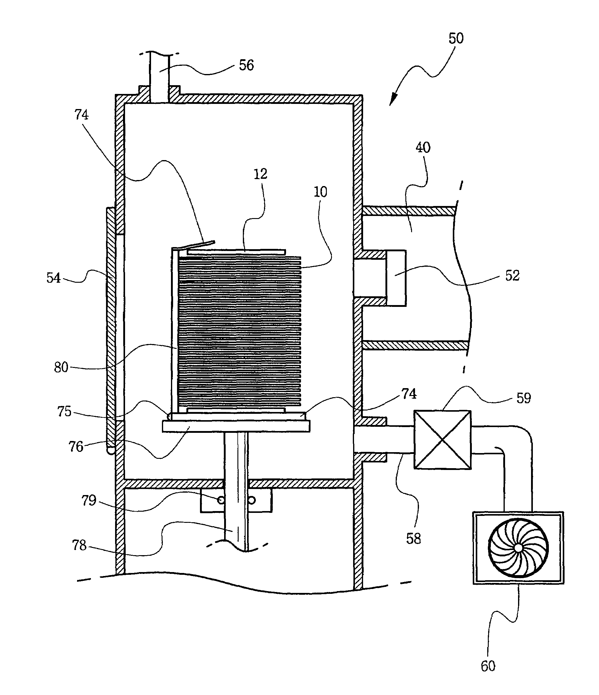
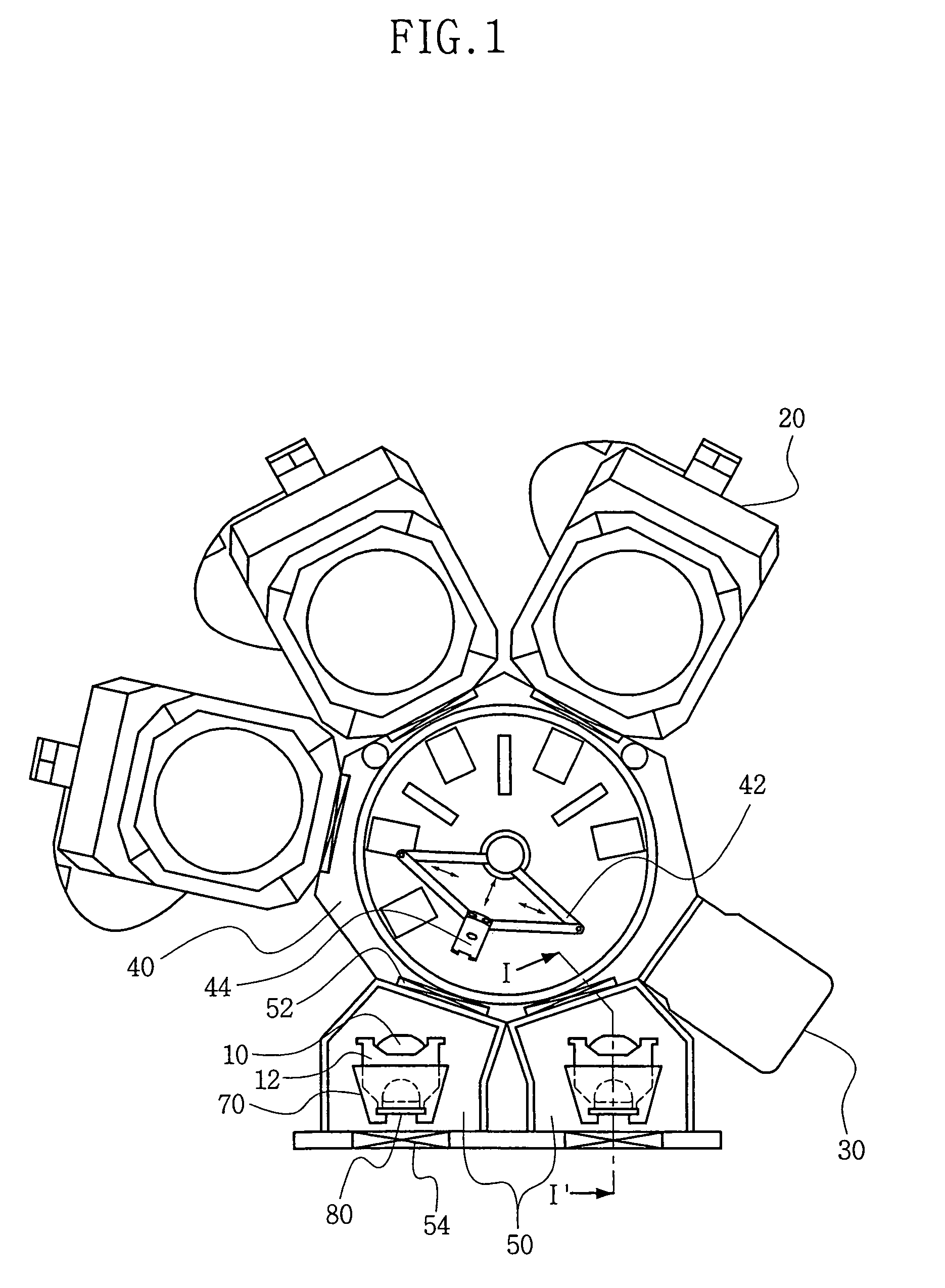
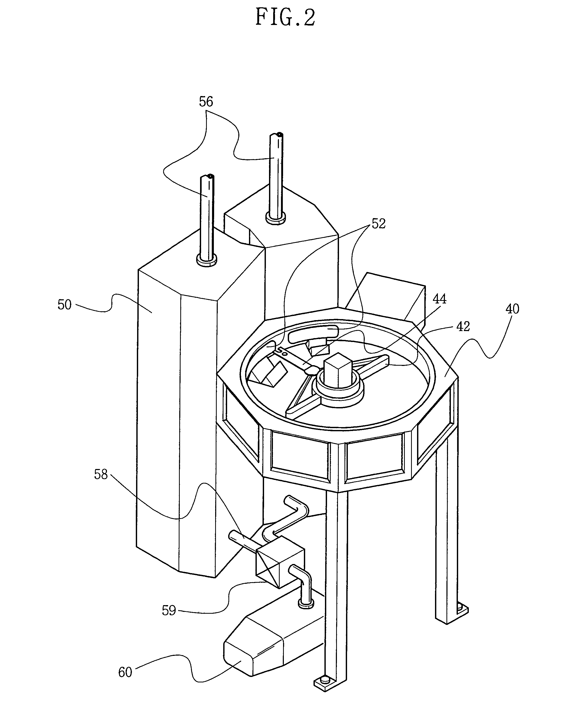
[0030]Referring to FIGS. 1 to 4, semiconductor device manufacturing equipment according to the present invention includes at least one process apparatus having a process chamber 20 in which a semiconductor manufacturing process is performed on at least one wafer 10 at a time, an alignment apparatus 30 that aligns the wafers 10 so that the flat zones of the wafers all face in one direction, at least one load-lock chamber 50, and a transfer chamber 40 in which a robot arm 42 is disposed for transferring the wafers 10 between the chambers. A slit valve 52 is interposed between one side of the load-lock chamber 50 and the transfer chamber 40. The slit valve 52, when opened, defines a passageway through which the robot arm 42 can pass to transfer a wafer from and / or back into the load-lock chamber 50. A door 54 is disposed at the side of the load-lock chamber 50 opposite the slit valve 52. The door 54 is large enough to allow a wafer cassette 12 to be transferred therethrough into and ou...

second embodiment

[0081]Now, the operation of the semiconductor manufacturing equipment in accordance with present invention will be described in more detail.

[0082]The door of the load-lock chamber 50 is opened. At this time, the cassette handler 70 is pivoted to its first (horizontal) position. At this time, the central duct of the ductwork 90 is flexed so as to extend horizontally along with the door 54. Then, a wafer cassette 12 is placed on the cassette handler 70 with the back of the wafer cassette 12 face down.

[0083]Subsequently, the cassette holder 70 is pivoted to the second (upright) position, as the door 54 is closed, to stand the wafer cassette 12 up in the load-lock chamber 50. At this time, the wafers 10 become oriented horizontally. Also, the central duct of the ductwork 90 extends vertically with the protrusion thereof facing the slit valve 50. Furthermore, the door 54 is coupled to and hermetically seals the rear wall of the load-lock chamber 50. Then the load-lock chamber 50 is evacu...


PUM

PropertyMeasurementUnit
pressureaaaaaaaaaa
vacuum pressureaaaaaaaaaa
corrosion-resistantaaaaaaaaaa

Abstract

A load-lock and semiconductor device manufacturing equipment have a wafer anti-contamination measure capable of maximizing production yield. The load-lock includes a chamber that can be hermetically sealed, a slit valve disposed at the front of the chamber for placing the chamber in communication with another chamber, a door disposed at the back of the chamber so as to allow a wafer cassette to be introduced into the chamber. In addition to having at least one of the load-locks, the semiconductor manufacturing equipment includes a transfer chamber to which the load-lock is connected, at least one process chamber connected to the transfer chamber, and an exhaust system by which each load-lock chamber is evacuated. The wafer anti-contamination measure may be an anti-eddy cover that covers the open back of a wafer cassette when the cassette is supported in the load-lock chamber. Alternatively, the wafer anti-contamination measure may be ductwork of the exhaust system that extends vertically along the door and / or rear wall of the load-lock chamber.

Description

BACKGROUND OF THE INVENTION[0001]1. Field of the Invention[0002]The present invention relates to semiconductor device manufacturing equipment. More particularly, the present invention relates to a load-lock and to semiconductor device manufacturing equipment having the same.[0003]2. Description of the Related Art[0004]Typically, a semiconductor device is fabricated by repetitively performing a series of processes, such as photolithography, diffusion, etching, deposition, and metallization processes, on a wafer. The manufacturing equipment for fabricating a semiconductor device includes apparatus for performing each of these processes. Therefore, semiconductor device manufacturing equipment typically includes etching, ion implantation, and deposition apparatus having processing chambers into which a wafer is loaded in a particular sequence. In this respect, the wafer must have a specific orientation relative to the apparatus or else the specific process is not performed with the nece...

Claims


Application Information

Patent Timeline
Patent Type & Authority Patents(United States)
IPC IPC(8): H01L21/677
CPCH01L21/67196H01L21/67201H01L21/67781H01L21/302
Inventor LEE, JIN-GOO
Owner SAMSUNG ELECTRONICS CO LTD
Why Eureka
Try Eureka