Method of separating semiconductor dies

a technology of semiconductor dies and dies, applied in the direction of semiconductor devices, basic electric elements, electrical equipment, etc., can solve the problems of presenting a challenge to the device handling during the separation process or in preparation of separation

Active Publication Date: 2008-11-18
SEMI PHOTONICS CO LTD
View PDF16 Cites 23 Cited by
  • Summary
  • Abstract
  • Description
  • Claims
  • Application Information

AI Technical Summary

Problems solved by technology

Due to the delicate nature of the unpackaged devices, handling the devices in preparation of separation or during the separation process presents a challenge.

Method used


Image

  • Method of separating semiconductor dies
  • Method of separating semiconductor dies
  • Method of separating semiconductor dies

Examples


Embodiment Construction

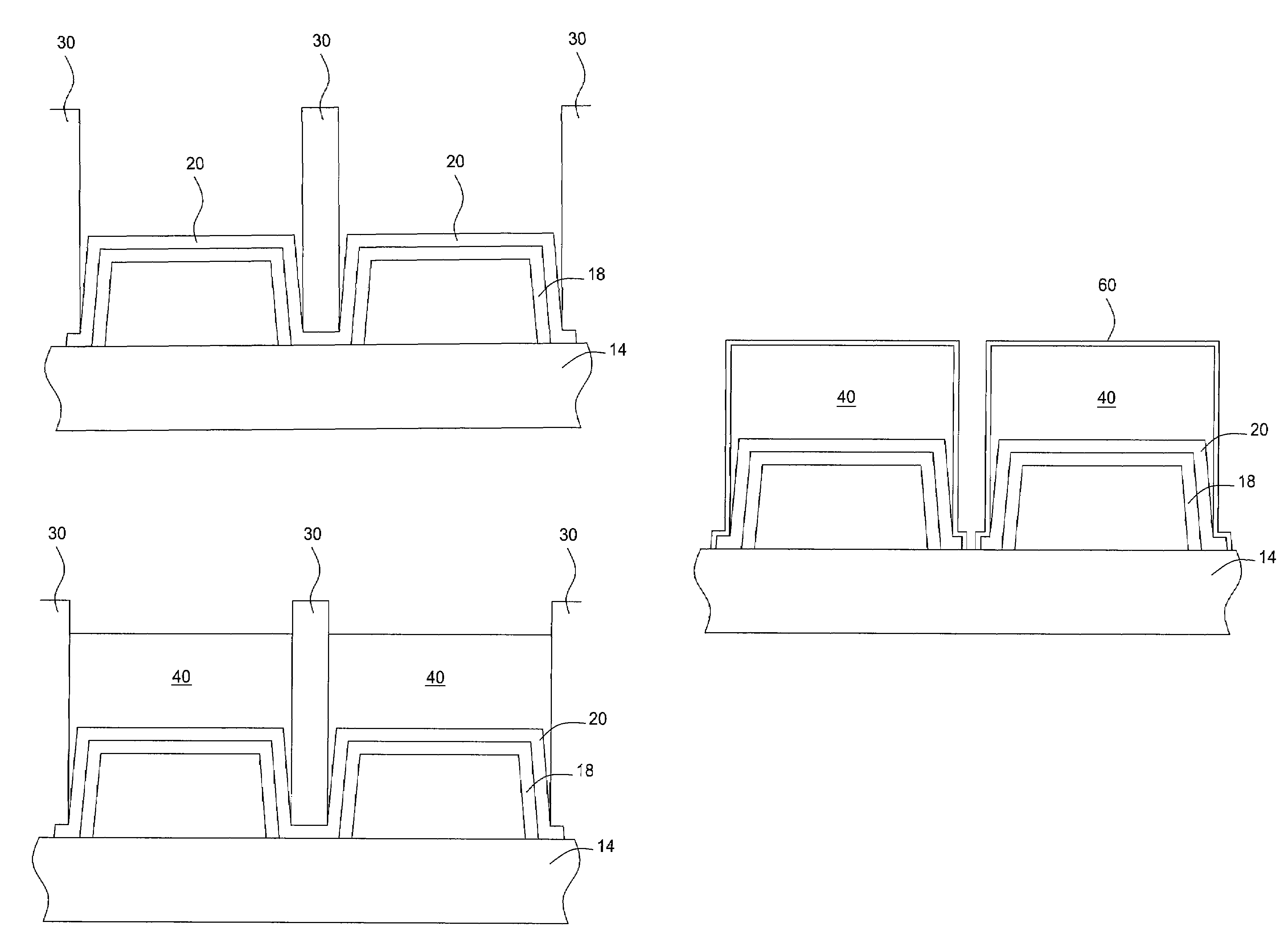
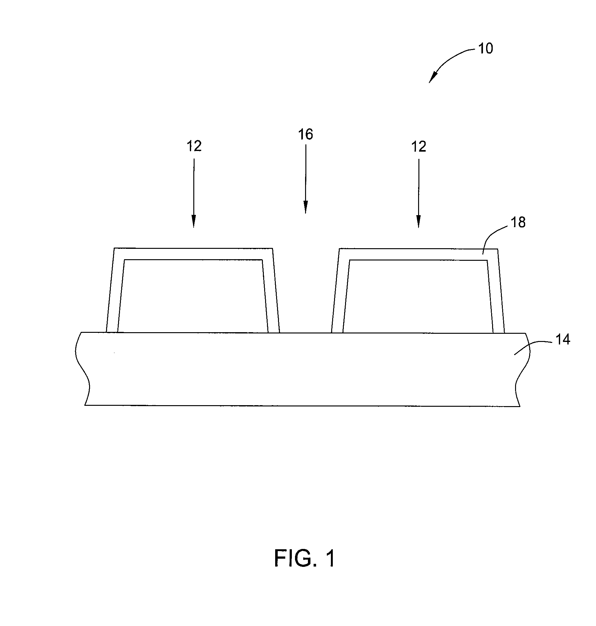
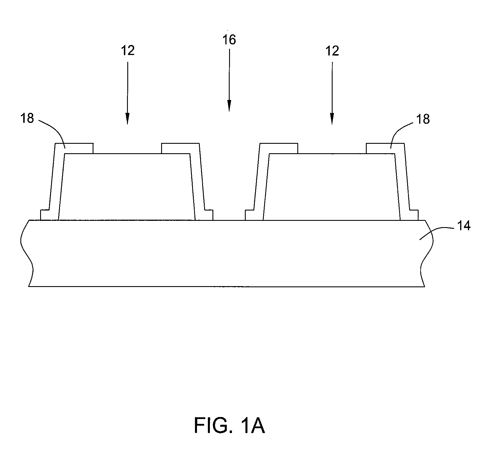
[0034]Embodiments of the present invention provide techniques and structures useful for separating multiple semiconductor dies present on a wafer. This method can be applied to any semiconductor wafer with multiple dies, and the case of separating multiple vertical light-emitting diode (VLED) dies is provided as an example. In the figures that follow, only two dies are shown, but this is representative of multiple dies on the entire wafer.

An Exemplary Method of Separating Semiconductor Dies

[0035]Referring now to FIG. 1, a generic multilayered semiconductor structure 10 is provided with two different dies 12 disposed on a substrate 14 and separated by a street section, or simply “the street”16. A passivation layer 18 may be deposited on the dies 12 with a portion of the passivation layer 18 removed as desired (e.g. for contact or grounding) for some embodiments as shown in FIG. 1A. The substrate 14 on which the dies 12 were formed may be composed of SiO2, sapphire, GaAs, InP, InGaAsP...


PUM

PropertyMeasurementUnit
thicknessaaaaaaaaaa
thicknessaaaaaaaaaa
thicknessaaaaaaaaaa

Abstract

A method for the separation of multiple dies during semiconductor fabrication is described. On an upper surface of a semiconductor wafer containing multiple dies, metal layers are deposited everywhere except where a block of stop electroplating material exists. The stop electroplating material is obliterated, and a barrier layer is formed above the entire remaining structure. A sacrificial metal element is added above the barrier layer, and then the substrate is removed. After the semiconductor material between the individual dies is eradicated, any desired bonding pads and patterned circuitry are added to the semiconductor surface opposite the sacrificial metal element, a passivation layer is added to this surface, and then the sacrificial metal element is removed. Tape is added to the now exposed barrier layer, the passivation layer is removed, the resulting structure is flipped over, and the tape is expanded to separate the individual dies.

Description

CROSS-REFERENCE TO RELATED APPLICATIONS[0001]This application claims benefit of U.S. Provisional Patent Application Ser. No. 60 / 780,896, filed Mar. 9, 2006, which is herein incorporated by reference.BACKGROUND OF THE INVENTION[0002]1. Field of the Invention[0003]Embodiments of the present invention generally relate to a method of semiconductor fabrication and, more particularly, to a method of separating multiple semiconductor dies.[0004]2. Description of the Related Art[0005]A wide variety of electronic devices, ranging from microprocessors to light-emitting diode (LED) structures, are typically formed in relatively large numbers as die on semiconductor wafer substrates. After formation, the devices must be separated for final packaging, typically via mechanical saw, “scribing and break,” or laser.[0006]In many cases, the devices must be placed on some type of device for final assembly, such as a tape allowing manipulation of the devices by a machine, such as a robot used in automa...

Claims


Application Information

Patent Timeline
Patent Type & Authority Patents(United States)
IPC IPC(8): H01L21/48
CPCH01L33/0079H01L33/0095H01L33/0093
Inventor CHU, CHEN-FUDOAN, TRUNG TRICHENG, HAO-CHUNFAN, FENG-HSUWANG, FU-HSIEN
Owner SEMI PHOTONICS CO LTD
Why Eureka
Try Eureka