

Three-dimensional face-to-face integration assembly
- Summary
- Abstract
- Description
- Claims
- Application Information
AI Technical Summary
Problems solved by technology
Method used
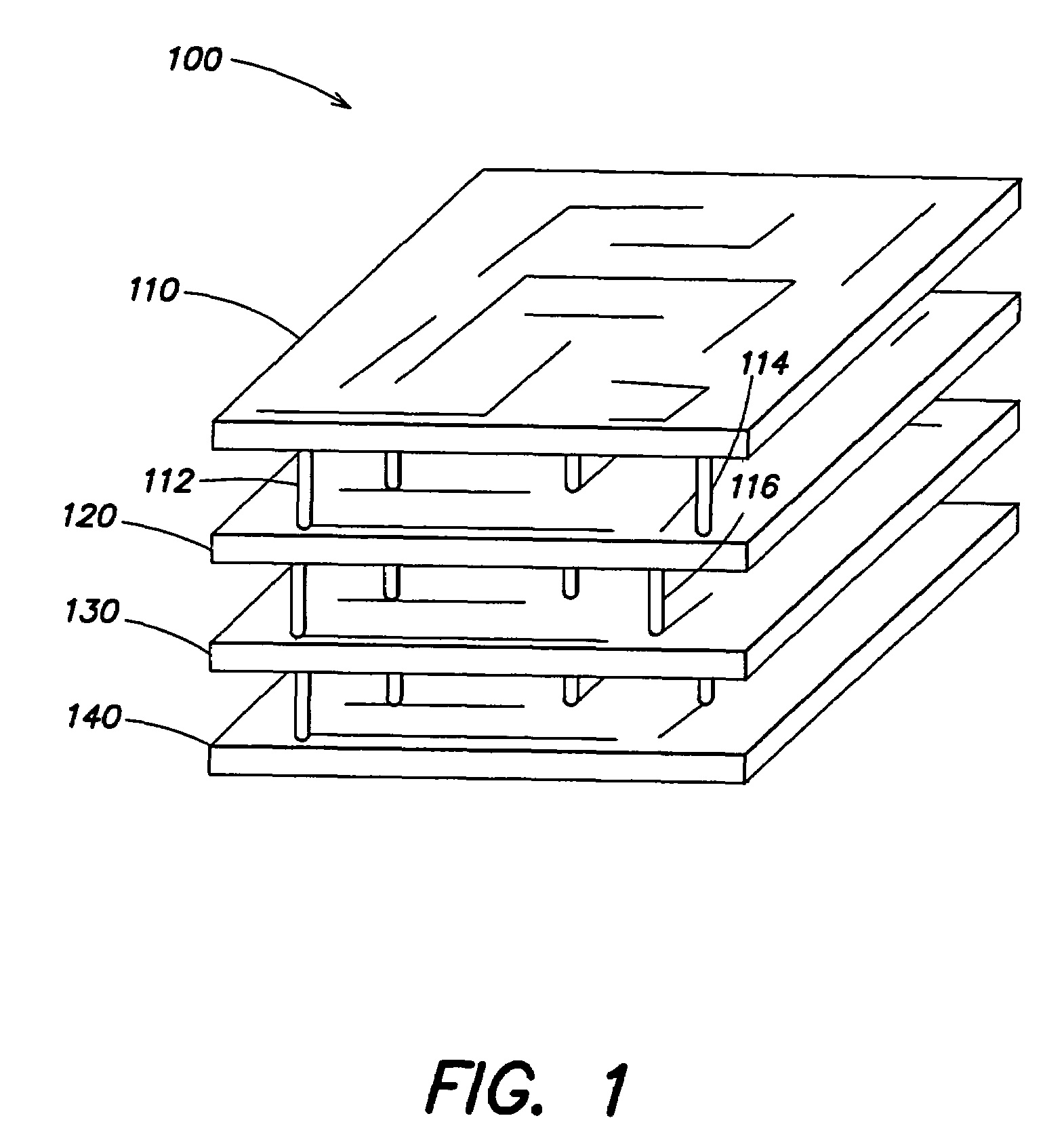
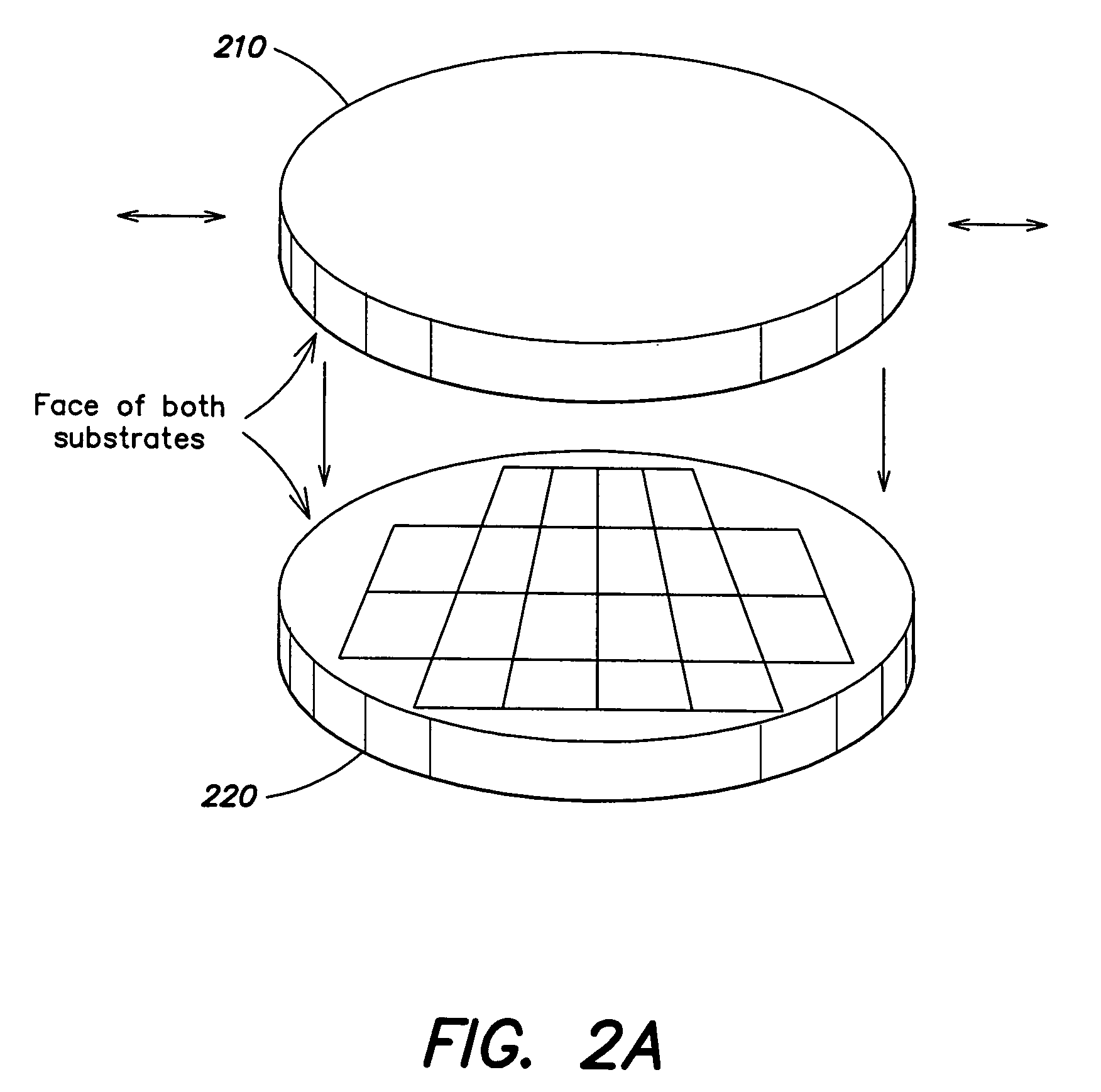
Image

Examples
Embodiment Construction
[0034]This invention is not limited in its application to the details of construction and the arrangement of components set forth in the following description or illustrated in the drawings. The invention is capable of other embodiments and of being practiced or of being carried out in various ways. Also, the phraseology and terminology used herein is for the purpose of description and should not be regarded as limiting. The use of “including,”“comprising,” or “having,”“containing”, “involving”, and variations thereof herein, is meant to encompass the items listed thereafter and equivalents thereof as well as additional items. In this application, the phrase “at least one of A and B” is equivalent to A and / or B, meaning A or B or (A and B).
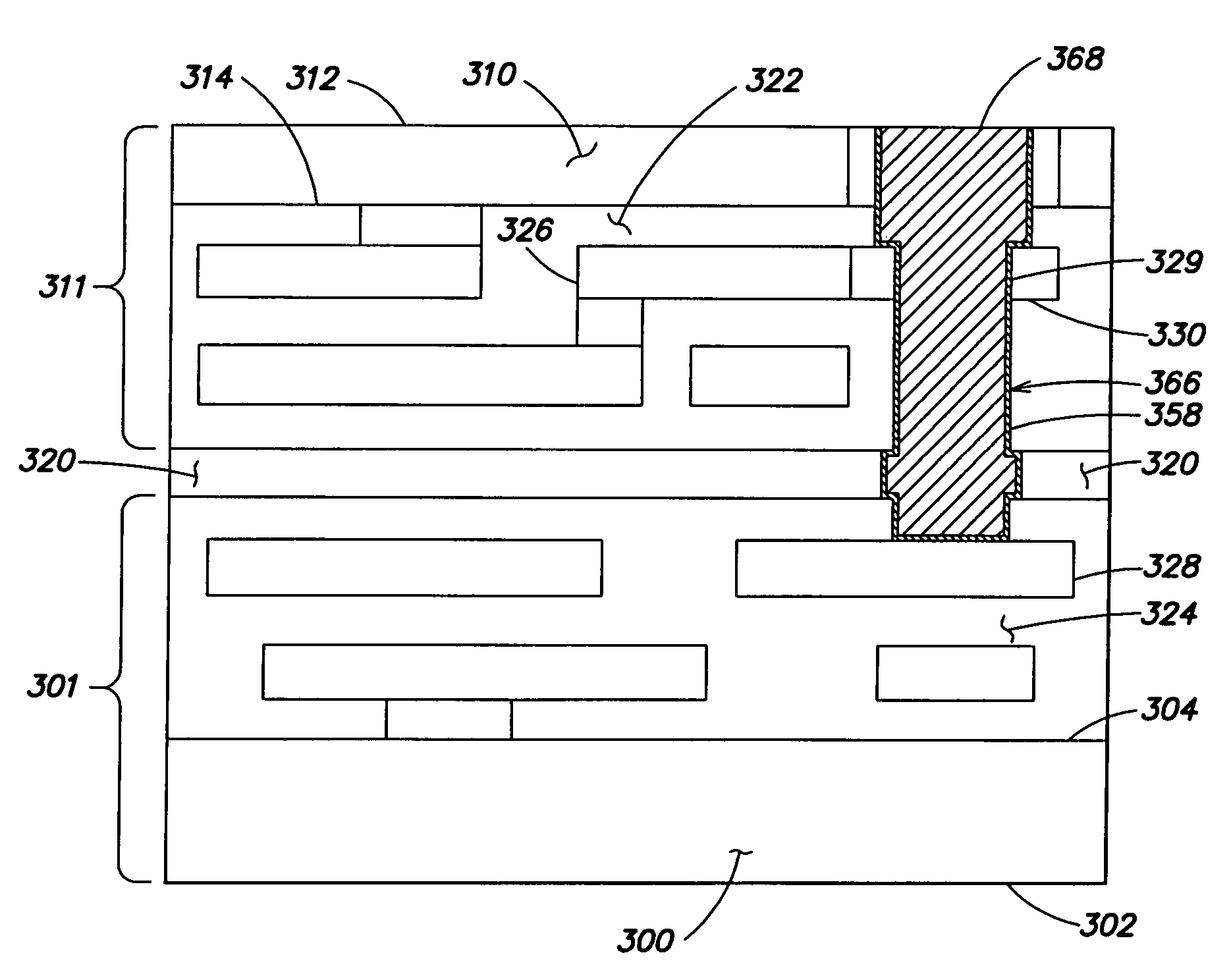
[0035]It should also be noted that in describing the semiconductor structures that follow, the term “on” will be used to describe the placement of devices, layers and features relative to each other. The term “on” in such situations is not meant t...
PUM
 Abstract
Description
Claims
Application Information