Semiconductor device and method of manufacturing the same

a semiconductor device and semiconductor technology, applied in the direction of semiconductor devices, semiconductor/solid-state device details, electrical apparatus, etc., can solve the problems of low modulus of elasticity, gold wires electrical short circuit, and inability to become sufficiently thin, so as to prevent electrical short circuit of wires and peeling of bump electrodes, maintain the modulus of elasticity of wires, and manufacture highly integrated semiconductor devices.

Inactive Publication Date: 2008-11-25
RENESAS ELECTRONICS CORP
View PDF11 Cites 104 Cited by
  • Summary
  • Abstract
  • Description
  • Claims
  • Application Information

AI Technical Summary

Benefits of technology

[0014]The features and advantages of the present invention may be summarized as follows. Since a wire can be cut with a low load, maintaining the modulus of elasticity o

Problems solved by technology

When performing stitch bonding of a gold wire on an aluminum pad on a chip directly, load of a capillary concentrates and a crack enters into SiO2 interlayer insulation film under the aluminum pad.
However, since the gold wire used as a material of bump electrode 14 is soft in the conventional formation of a bump electrode with a gold wire and conventional stitch bonding of a gold wire onto a bump electrode, crush of gold wire 13 held by capillary 12 and bump electrode 14 b

Method used


Image

  • Semiconductor device and method of manufacturing the same
  • Semiconductor device and method of manufacturing the same
  • Semiconductor device and method of manufacturing the same

Examples


first embodiment

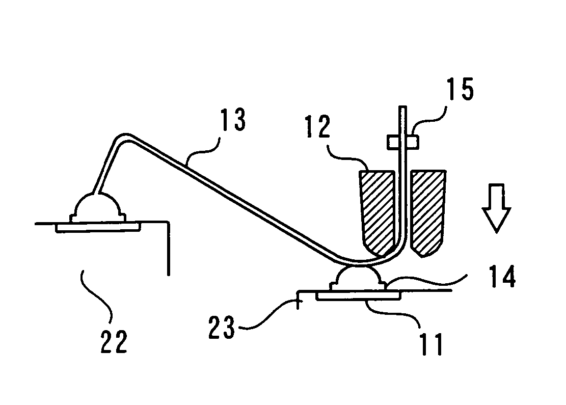
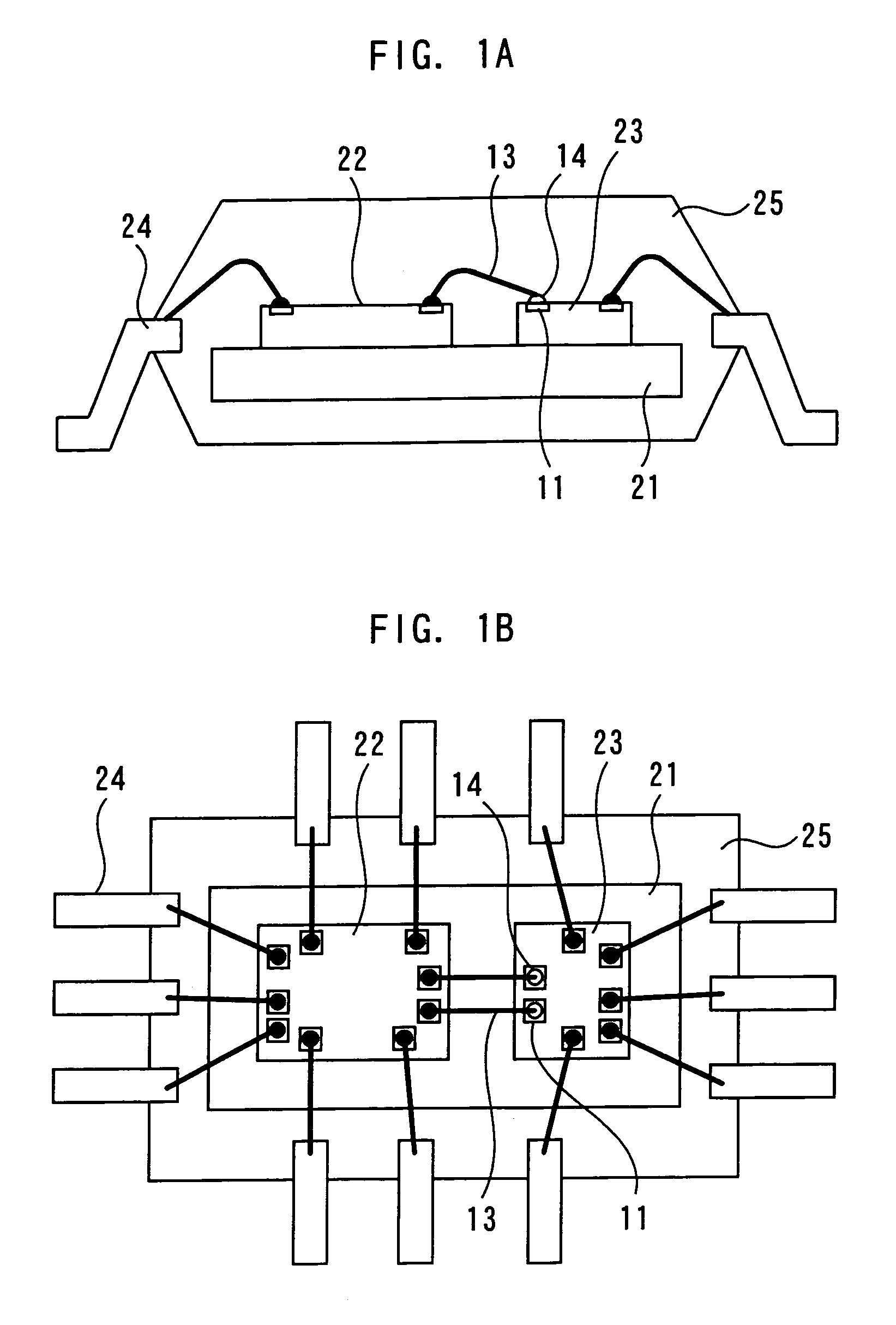
[0029]FIG. 1A is a sectional view showing an example of the semiconductor device concerning First Embodiment of the present invention, and FIG. 1B is the top view. Chip 22 and chip 23 are mounted on die pad 21, being put in order. These chips 22 and 23 and lead 24 are connected by gold wire 13. Further, bump electrode 14 is formed on aluminum pad 11 of chip 23. And ball bonding of the gold wire 13 is performed on the aluminum pad of chip 22, and the stitch bonding is performed on bump electrode 14. Furthermore, the whole is sealed with sealing resin 25.

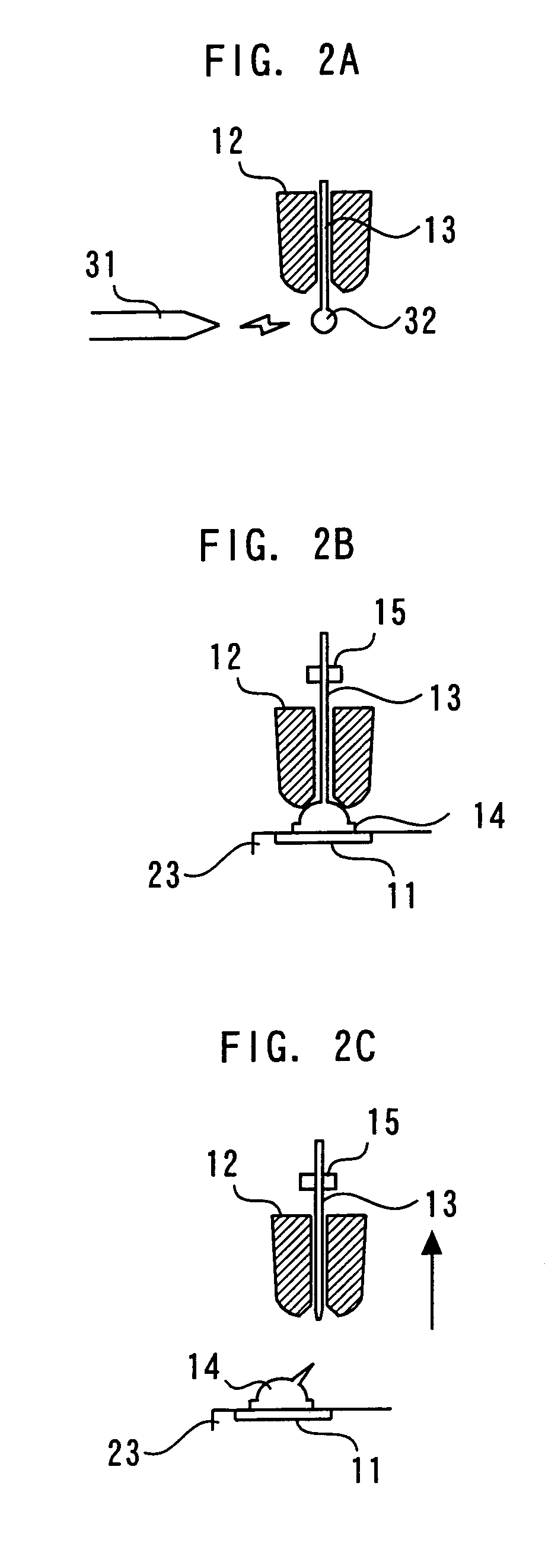
[0030]FIGS. 2A-2C are sectional views showing the step which forms a bump electrode. First, as shown in FIG. 2A, gold ball 32 with a larger diameter than gold wire 13 is formed by melting the tip of gold wire 13 discharged from capillary 12 by discharge from blowpipe 31. Then, as shown in FIG. 2B, gold ball 32 is pushed and pressed by capillary 12 on aluminum pad 11 of chip 23 arranged on a stage. And the interface of aluminum pad 11 ...

second embodiment

[0042]FIGS. 8A-8D are sectional views showing a manufacturing method of the semiconductor device concerning Second Embodiment of the present invention. First, as shown in FIG. 8A, bump electrode 14 is formed by joining the gold ball at the tip of gold wire 13 discharged from capillary 12 on aluminum pad 11 of chip 23, However, the thing of the material same as gold wire 13 as First Embodiment is used.

[0043]And as shown in FIG. 8B, capillary 12 is raised by 15 μm. Here, since the height of bump electrode 14 is 15 μm, capillary 12 is evacuated above bump electrode 14. In the dimension of capillary 12 and gold wire 13 which are used in the embodiment, the inside diameter of capillary 12 is 30 μm, and the diameter of gold wire 13 is 23 μm.

[0044]Capillary 12 is made to reciprocate in a horizontal direction after that, as shown in FIG. 8C. However, the operational amplitude of capillary 12 is more than the clearance between gold wire 13, and the inner wall of capillary 12 at least. Since ...

third embodiment

[0048]FIGS. 9A-9D are sectional views showing a manufacturing method of a semiconductor device concerning Third Embodiment of the present invention. First, as shown in FIG. 9A, after performing ball bonding of the gold ball at gold wire 13 tip on the aluminum pad of chip 22 using capillary 12, stitch bonding of the gold wire 13 is performed on bump electrode 14 formed on aluminum pad 11 of chip 23. Concretely speaking, gold wire 13 is crushed pushing and pressing gold wire 13 for 10 ms to bump electrode 14 by capillary 12, and applying supersonic vibration, and gold wire 13 is joined to bump electrode 14. However, as gold wire 13, the thing of the same material as First Embodiment is used.

[0049]After that, as shown in FIG. 9B, capillary 12 is evacuated more than half of the amplitude of the horizontal direction action of capillary 12 of later process in the loop advancement direction of gold wire 13. For example, horizontal displacement of the capillary 12 is performed by 30 μm.

[005...


PUM


Abstract

A semiconductor device of the present invention includes a chip which has a pad; a bump electrode formed on the pad; and a wire whose stitch bonding is made on the bump electrode. The wire satisfies a condition: (modulus-of-elasticity/breaking strength per unit area) ≧400.

Description

BACKGROUND OF THE INVENTION[0001]1. Field of the Invention[0002]The present invention relates to a semiconductor device having a chip which has a pad, a bump electrode formed on the pad, and a wire whose stitch bonding is performed on the bump electrode, and its manufacturing method.[0003]2. Background Art Background Art[0004]When performing stitch bonding of a gold wire on an aluminum pad on a chip directly, load of a capillary concentrates and a crack enters into SiO2 interlayer insulation film under the aluminum pad. For this reason, a bump electrode is used for the wire bonding between a chip and a chip (chip-to-chip) (for example, refer to Japanese Unexamined Patent Publication No. 2001-15541). Further, in a thin package, in order to make the height of a gold wire low, reverse bonding using a bump electrode is performed.[0005]FIGS. 10A and 10B are sectional views showing the state of conventional bump electrode formation. First, as shown in FIG. 10A, bump electrode 14 is formed...

Claims


Application Information

Patent Timeline
IPC IPC(8): H01L21/44
CPCH01L23/3128H01L23/4952H01L23/49575H01L24/05H01L24/06H01L24/45H01L24/48H01L24/49H01L24/85H01L25/0657H01L2224/48624H01L2224/05554H01L2224/49175H01L2224/49433H01L2224/78301H01L2224/85051H01L2224/85121H01L2224/85205H01L2224/85986H01L2225/0651H01L2225/06575H01L2924/01004H01L2924/01005H01L2924/01013H01L2924/0105H01L2924/01079H01L2924/01082H01L2924/014H01L2924/15311H01L2924/20752H01L2224/49171H01L2924/01033H01L2924/01006H01L2224/48479H01L2224/48471H01L2224/48465H01L2224/48247H01L2224/48137H01L2224/48091H01L2224/45144H01L2224/45015H01L2224/32145H01L2224/06136H01L24/78H01L2224/04042H01L2224/05624H01L2924/00014H01L2224/85186H01L2224/48227H01L2924/00H01L2924/00011H01L2924/181H01L2224/78621H01L2924/00015H01L2924/00012H01L2224/4554
Inventor KURAYA, HIDETOSHIARAKAWA, HIDEYUKIAGA, FUMIAKI
Owner RENESAS ELECTRONICS CORP
Why Eureka
Try Eureka