Coated article with ion treated underlayer and corresponding method

a technology of ion treatment and coating article, which is applied in the direction of vacuum evaporation coating, electric/magnetic/electromagnetic heating, transportation and packaging, etc., can solve the problems of undesirable drop in visible transmission, undesirable color shift of product, and difficult to obtain high visible transmission and adequate solar control properties. , to achieve the effect of less structural defects, less reactive, and less sodium migration

Inactive Publication Date: 2005-12-29
GUARDIAN GLASS LLC
View PDF34 Cites 44 Cited by
  • Summary
  • Abstract
  • Description
  • Claims
  • Application Information

AI Technical Summary

Benefits of technology

[0013] Surprisingly, it has been found that this excess nitrogen in the layer (i.e., due to the N-doping of Si3N4) is advantageous in that it results in less structural defects, reduced sodium migration during optional heat treatment when used in a layer under an IR reflecting layer(s), and renders the layer less reactive to oxygen thereby improving durability characteristics.
[0014] In certain example embodiments of this invention, at least nitrogen (N) ions are used to ion treat a layer comprising silicon nitride. In certain example embodiments, using an ion beam treatment post-sputtering (i.e., peening), such an ion beam treatment may include utilizing an energy of at least about 550 eV per N2+ ion, more preferably from about 550 to 1,200 eV per N2+ ion, even more preferably from about 600 to 1100 eV per N2+ ion, and most preferably from about 650 to 900 eV per N2+ ion (an example is 750 eV per N2+ ion). It has surprisingly been found that such ion energies permit excellent nitrogen grading characteristics to be realized in a typically sputter-deposited layer of suitable thickness, significantly reduce the number of dangling Si bonds at least proximate the surface of the layer comprising silicon nitride, provide improved stress characteristics to the coating / layer, provide excellent doping characteristics, reduce the potential for sodium migration, and / or cause part or all of the layer to become nitrogen-rich (N-rich) which is advantageous with respect to durability. Possibly, such post-sputtering ion beam treatment may even cause the stress of the layer to change from tensile to compressive in certain example instances.
[0015] In IBAD embodiments where the ion beam treatment is performed simultaneously with sputtering of the layer, it has surprisingly been found that a lower ion energy of at least about 100 eV per N2+ ion, more preferably of from about 200 to 1,000 eV per N2+ ion, more preferably from about 200 to 600 eV per N2+ ion, still more preferably from about 300 to 500 eV per N2+ ion (example of 400 eV per N2+ ion) is most suitable at the surface being treated. It has surprisingly been found that such ion energies in IBAD embodiments significantly reduce the number of dangling Si bonds, provide improved stress characteristics to the coating / layer, provide excellent doping characteristics, reduce sodium migration during heat treatment, and / or cause part or all of the layer to become nitrogen-rich (N-rich) which is advantageous with respect to durability.
[0016] In certain example embodiments, the use of ion treatments herein may speed up the manufacturing process by permitting faster speeds to be used in sputter depositing certain layer(s) of a coating without suffering from significant durability problems.

Problems solved by technology

It is often difficult to obtain high visible transmission and adequate solar control properties, combined with good durability because materials used to improve durability often cause undesirable drops in visible transmission and / or undesirable color shifts of the product upon heat treatment.
However, a problem which frequently occurs with heat treatment is sodium (Na) migration into the coating from the glass substrate.
For instance, during heat treatment (HT) sodium tends to migrate from the glass substrate into the coating and can severely damage the infrared (IR) reflecting layer(s) (e.g., silver layer or layers) if such migrating sodium reaches the same.
However, silicon nitride formed only by sputtering is problematic in certain respects. FIG. 1 of the instant application, for example, illustrates that sputter-deposited silicon nitride layers realize an increase in voids defined therein as sputter deposition rate increases (the data in FIG. 1 is from silicon nitride deposited only via sputtering in a known manner).
A large number of voids in a base layer of silicon nitride can be undesirable since sodium can migrate through the layer during heat treatment via such voids, and attack the IR reflecting layer(s) leading to structural damage and / or coating failure.
For example, such sodium attacks can increase haze in the heat treated coated article and / or can adversely affect optical characteristics of the coated article following heat treatment.
However, the '362 patent is unrelated to nitrogen doping Si3N4, is unrelated to heat treated products and problems which may arise upon heat treatment, and is undesirable in that it's use of significant amounts of oxygen in the ion beam renders treated layers and layers adjacent thereto susceptible to significant undesirable change upon heat treatment.

Method used


Image

  • Coated article with ion treated underlayer and corresponding method
  • Coated article with ion treated underlayer and corresponding method
  • Coated article with ion treated underlayer and corresponding method

Examples


examples 1-3

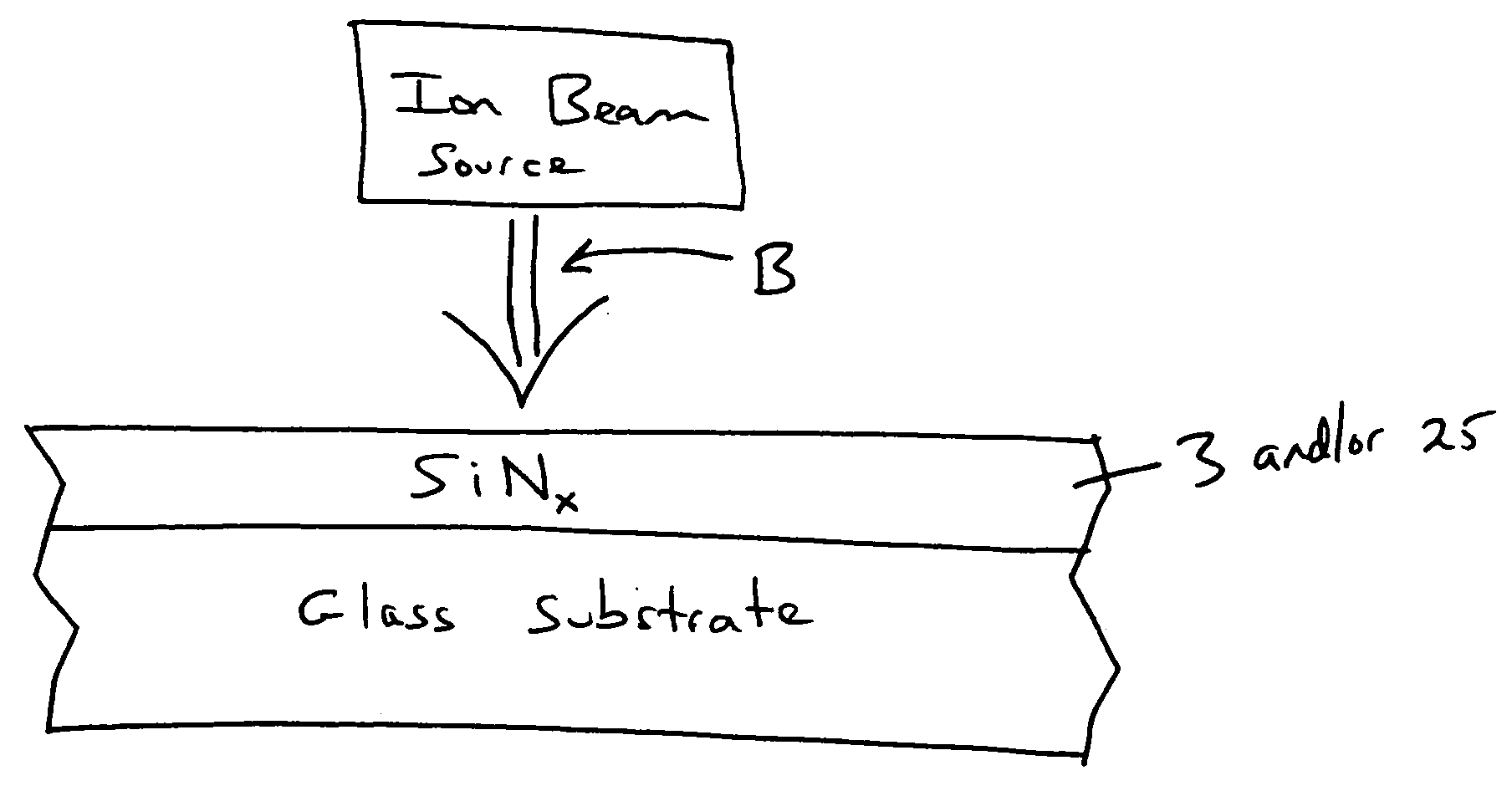
[0078] Examples 1-3 illustrate example techniques for forming layers 3 and / or 25, or any other suitable layer according to example embodiments of this invention. Examples 1-3 utilized IBAD type of ion beam treatment, and were made and tested as follows. A silicon nitride layer was deposited on a quartz wafer (used for ease of stress testing) using IBAD (e.g., see FIG. 8) under the following conditions in the deposition chamber: pressure of 2.3 mTorr; anode / cathode ion beam source voltage of about 800 V; Ar gas flow in the ion source of 15 sccm; N2 gas flow in the ion source 26 of 15 sccm; sputtering target of Si doped with about 1% boron; 460 V applied to sputtering cathode; 5.4 sputtering amps used; 60 sccm Ar and 40 sccm N2 gas flow used for sputtering gas flow; linear line speed of 50 inches / minute; where the quartz wafer substrate was circular in shape and about 0.1 to 0.15 mm thick. The ion beam treatment time for a given area was about 3 seconds.

[0079] Example 2 was the same ...

example 4

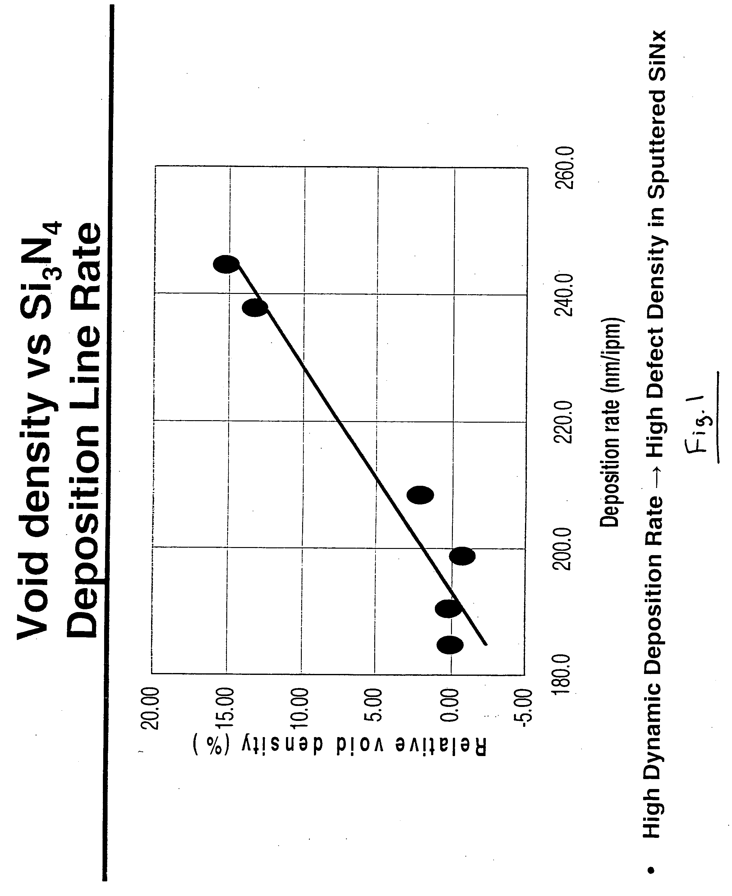
[0083] Example 4 used post-sputtering peening type of ion beam treatment, and was made and tested as follows. A silicon nitride layer about 425 Å thick was deposited by conventional magnetron-type sputtering using a Si target doped with Al on a substrate. After being sputter-deposited, the silicon nitride layer had a tensile stress of 400 MPa as tested on the quartz wafer. After being sputter-deposited and stress tested, the silicon nitride layer was ion beam treated using an ion source 26 as shown in FIGS. 6-7 under the following conditions: ion energy of 750 eV per N ion; treatment time of about 18 seconds (3 passes at 6 seconds per pass); and N2 gas used in the ion source. After being ion beam treated, the silicon nitride layer was again tested for stress, and had a tensile stress of only 50 MPa. Thus, the post-sputtering ion beam treatment caused the tensile stress of the silicon nitride layer to drop from 400 MPa down to 50 MPa (a drop of 87.5%).

example 5

[0084] The following hypothetical Example 5 is provided for purposes of example only and without limitation, and uses a 2.1 mm thick clear glass substrates so as to have approximately the layer stack set forth below and shown in FIG. 3. The layer thicknesses are approximations, and are in units of angstroms (A).

Layer Stack for Example 5

[0085]

LayerGlass SubstrateThickness (Å)N-doped Si3N4100ZnAlOx109Ag96NiCrOx25SnO2535SixNy126ZnAlOx115Ag95NiCrOx25SnO2127N-doped Si3N4237

[0086] The processes used in forming the coated article of Example 5 are set forth below. The sputtering gas flows (argon (Ar), oxygen (O), and nitrogen (N)) in the below table are in units of sccm (gas correction factor of about 1.39 may be applicable for argon gas flows herein), and include both tuning gas and gas introduced through the main. The line speed was about 5 m / min. The pressures are in units of mbar x 10−3. The silicon (Si) targets, and thus the silicon nitride layers, were doped with aluminum (Al). The Z...


PUM

PropertyMeasurementUnit
compressive stressaaaaaaaaaa
sheet resistanceaaaaaaaaaa

Abstract

A coated article is provided that may be used as a vehicle windshield, insulating glass (IG) window unit, or the like. Ion beam treatment is performed on a layer(s) of the coating. For example, a silicon nitride layer of a low-E coating may be ion beam treated. It has been found that ion beam treatment, for example, of a silicon nitride underlayer is advantageous in that sodium migration from the glass substrate toward the IR reflecting layer(s) can be reduced during heat treatment.

Description

[0001] This invention relates to a coated article including a solar control coating such as a low-E coating. In certain example embodiments, the low-E coating includes a layer (e.g., an undercoat layer) which is ion treated. In certain example embodiments, an undercoat layer comprising silicon nitride is ion beam treated simultaneously with sputtering. Coated articles according to certain example embodiments of this invention may be used in the context of vehicle windshields, insulating glass (IG) window units, other types of windows, or in any other suitable application. BACKGROUND OF THE INVENTION [0002] Coated articles are known in the art for use in window applications such as insulating glass (IG) window units, vehicle windows, and / or the like. Example non-limiting low-emissivity (low-E) coatings are illustrated and / or described in U.S. Pat. Nos. 6,723,211; 6,576,349; 6,447,891; 6,461,731; 3,682,528; 5,514,476; 5,425,861; and 2003 / 0150711, the disclosures of which are all hereb...

Claims


Application Information

Patent Timeline
Patent Type & Authority Applications(United States)
IPC IPC(8): C03C17/34C03C17/36C03C23/00
CPCC03C17/3435C03C17/36C03C17/3626C03C17/3644Y10T428/26C03C23/0055C03C2217/78C03C2218/326Y10T428/315C03C17/366
Inventor VEERASAMY, VIJAYEN S.
Owner GUARDIAN GLASS LLC
Why Eureka
Try Eureka