Method for forming semiconductor devices having reduced gate edge leakage current

a technology of gate edge leakage current and semiconductor device, which is applied in the field of improved semiconductor gate dielectric and field effect transistor (fet) processing, can solve the problems of poor dielectric or device reliability at or near the edges of fet device, high gate leakage current, gate dielectric,

Active Publication Date: 2008-11-25
TAIWAN SEMICON MFG CO LTD
View PDF5 Cites 9 Cited by
  • Summary
  • Abstract
  • Description
  • Claims
  • Application Information

AI Technical Summary

Problems solved by technology

Thinner gate dielectrics typically cause higher gate leakage currents due to increased tunneling, which has the undesired effect of increasing power dissipation in CMOS integrated circuits.
However, as gate length is reduced, the edge component contributes increasingly more, and can even dominate the total gate leakage current.
During an overetch process to ensure that the gate electrode is completely etched away, edge regions of the gate dielectric 120 are exposed to the RIE, which can damage the gate dielectric and result in poor dielectric or device reliability at or near the edges of FET device 100.
The high temperature nitridation and thermal re-oxidation processing steps described in the '344 Patent can lead to various problems such as n-FET (n-type FET device) polysilicon profile degradation, dopant loss (e.g. phosphorous dopant loss), and thermal-induced gate oxide defects.
Thus, if the polysilicon gate is not uniformly doped at the time of re-oxidation, the oxide will grow to a different thickness along the vertical surface of the gate, resulting in a non-optimal polysilicon gate profile.
Additionally, the high thermal budget for a high temperature re-oxidation process is known to degrade gate dielectric yield.
Reductions in both gate conductor length and gate dielectric thickness are needed to increase FET device performance, however, both techniques exasperate parasitic gate edge leakage currents.
This is especially true for low power applications where gate edge leakage is a major component of power dissipation.

Method used


Image

  • Method for forming semiconductor devices having reduced gate edge leakage current
  • Method for forming semiconductor devices having reduced gate edge leakage current
  • Method for forming semiconductor devices having reduced gate edge leakage current

Examples


Embodiment Construction

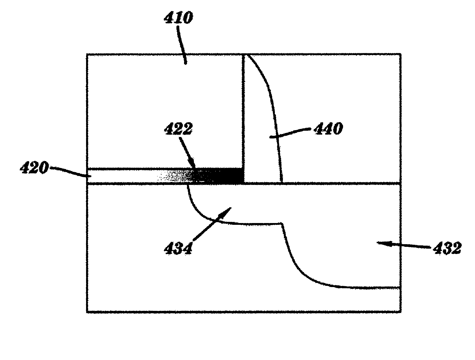
[0020]The present invention provides methods for forming FET devices that have reduced or suppressed the aforementioned problems by processing the gate stack of the FET devices in accordance with low temperature nitridation and plasma re-oxidation processes, and FET devices and circuits formed in accordance therefrom.

[0021]A method of carrying out the present invention is illustrated in FIGS. 3A-3G, which are cross-sectional views of a semiconductor device at various stages of the method. Semiconductor substrate 310 is provided for forming n-FET and / or p-FET type devices as shown in FIG. 3A. Substrate 310 can comprise any suitable semiconductor material such as silicon, bulk silicon, silicon-on-insulator (“SOI”), SiGe, Ge, GaAs, or the like.

[0022]With reference to FIG. 3B, an insulating layer 312 is formed on an upper surface of substrate 310. For example, insulating layer 312 can be deposited or grown on the substrate. Insulating layer 312 can comprise normal-k insulative materials...


PUM


Abstract

The present invention provides methods for forming semiconductor FET devices having reduced gate edge leakage current by using plasma or thermal nitridation and low-temperature plasma re-oxidation processes post gate etch.

Description

FIELD OF THE INVENTION[0001]The present invention broadly relates to semiconductor processing, and more particularly, to improved semiconductor gate dielectric and Field Effect Transistor (FET) processing.DESCRIPTION OF THE PRIOR ART[0002]Transistor scaling is one of many conventional techniques for improving semiconductor circuit performance. Complimentary-Metal-Oxide-Semiconductor (CMOS) transistor scaling conventionally includes the reduction of polysilicon gate length and gate insulator thickness to smaller dimensions to increase transistor drive current. Reduction of polysilicon gate length is conventionally done in conjunction with FET gate dielectric thinning to improve short-channel effects by increasing gate control of the channel.[0003]Thinner gate dielectrics typically cause higher gate leakage currents due to increased tunneling, which has the undesired effect of increasing power dissipation in CMOS integrated circuits. Tunneling is a current leakage mechanism whereby le...

Claims


Application Information

Patent Timeline
Patent Type & Authority Patents(United States)
IPC IPC(8): H01L21/31
CPCH01L21/28176H01L29/512H01L29/518H01L29/517H01L29/7833
Inventor CHOU, ANTHONY I-CHIHNARASIMHA, SHREESH
Owner TAIWAN SEMICON MFG CO LTD
Why Eureka
Try Eureka