Integrated circuit chip and integrated device

a technology of integrated circuits and integrated devices, which is applied in the direction of semiconductor devices, semiconductor device details, electrical apparatus, etc., can solve the problems of increasing the power supply system noise, limiting the performance of high-speed memory packages, and the electric performance of integrated devices becoming a limiting factor in high-speed memory packages, etc., to increase the probability of shorts

Inactive Publication Date: 2008-11-25
QIMONDA
View PDF9 Cites 23 Cited by
  • Summary
  • Abstract
  • Description
  • Claims
  • Application Information

AI Technical Summary

Benefits of technology

[0011]One benefit of the integrated circuit chip according to at least one embodiment of the present invention is that when bonding the signal pad and the power supply pad with bond wires in a direction substantially perpendicular to the extension of the pad rows, the bond wires can be led closer to each other in comparison to bond wires connected to adjacent pads of one pad row which have to be spaced apart by a minimum pad spacing distance. The integrated circuit chip according to this embodiment of the present invention allows the reduction of the spacing between the bond wires for the signal and for the power / ground supply. As the bond wires for the signal pad and for the power supply pad result in a common loop inductance which is affected by the spacing of the bond wires of their length, this reduction in spacing results in a reduced signal-to-supply loop inductance which substantially improves the high frequency signal transmission over the signal bond wire.
[0013]Various relative arrangements of the signal pad and associated power supply pads are contemplated. For example, in one arrangement the pads in the first and second rows are arranged in a substantially linear pattern and the two or more associated power supply pads (in the second row) for a given signal pad (in the first row) may be adjacent to one another. In one embodiment, the pads of the first and second pad rows are arranged in a staggered condition relative to each other. Further, the associated power supply pads may be those pads of the second pad row that are closest to the signal pad in the first pad row. The staggered arrangement of the pads allows for associating two supply pads to the signal pad such that corresponding supply bond wires may both be spaced from the signal bond wire with substantially the same distance.
[0017]In one embodiment, the integrated device provides an integrated circuit chip which is connected to respective contact elements via bond wires. Due to the pad arrangement on the substrate, the bond wires are spaced apart with a reduced distance compared to the bond wires being connected to adjacent pads in a single pad row which are spaced apart as predetermined by the pad pitch of the pads in the pad row. The reduced spacing between the bond wires reduces the signal-to-power-supply loop inductance in such a way that the high frequency signal transmission to and from the integrated circuit can be improved.
[0019]The power supply contact element and the signal contact element may each be arranged in respective contact element rows which correspond to or mirror the arrangement of the pads of the first and second pad rows. This is to avoid bond wires crossing each other which would increase the probability of shorts.

Problems solved by technology

The electrical performance of integrated devices increasingly develops into a limiting factor in high-speed memory packages, e.g. for graphics applications.
One of the main issues is the noise generated by the non-ideal power supply system.
Although the loop inductance can be minimized and the required impedance of the package can be achieved by means of routing measures, the bonding wires within the package seem to limit the high frequency package performance.
Dual slot FBGA packages reduce the length of bonding wires for power supply planes, but with today's pad arrangement on the chip the inductance of the signal bond wires and the signal-to-power coupling within the bond wire region cannot be affected significantly.
Moreover, the distance between the signal and the supply bond wires is limited by the pad pitch and cannot be reduced by shrinking the feature sizes due to restrictions of the bonding equipment.
Consequently, the result is an impedance discontinuity of bond wires which can only be minimized by shortening the bond wires wherever possible.
However, this approach leads to increased packaging costs.

Method used


Image

  • Integrated circuit chip and integrated device
  • Integrated circuit chip and integrated device
  • Integrated circuit chip and integrated device

Examples


Embodiment Construction

[0035]In the following, reference is made to embodiments of the invention. However, it should be understood that the invention is not limited to specific described embodiments. Instead, any combination of the following features and elements, whether related to different embodiments or not, is contemplated to implement and practice the invention. Furthermore, in various embodiments the invention provides numerous advantages over the prior art. However, although embodiments of the invention may achieve advantages over other possible solutions and / or over the prior art, whether or not a particular advantage is achieved by a given embodiment is not limiting of the invention. Thus, the following aspects, features, embodiments and advantages are merely illustrative and, unless explicitly present, are not considered elements or limitations of the appended claims.

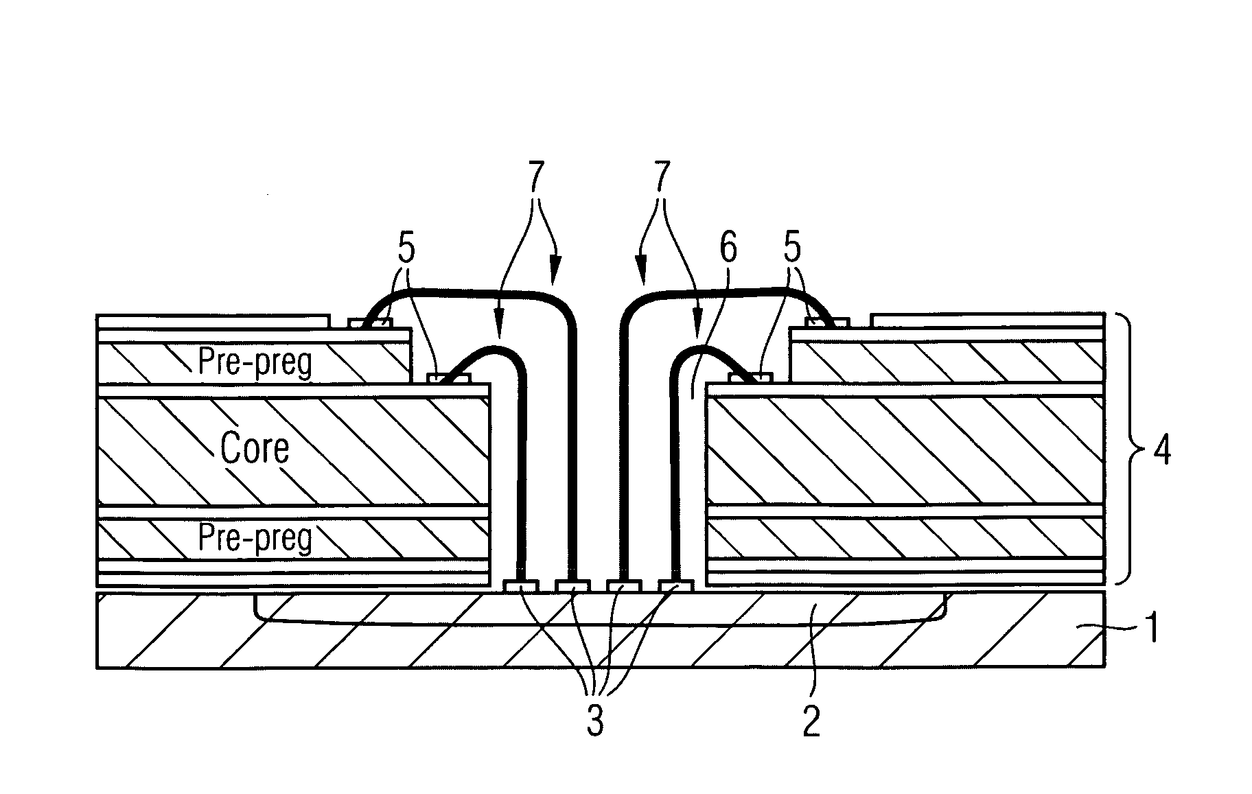
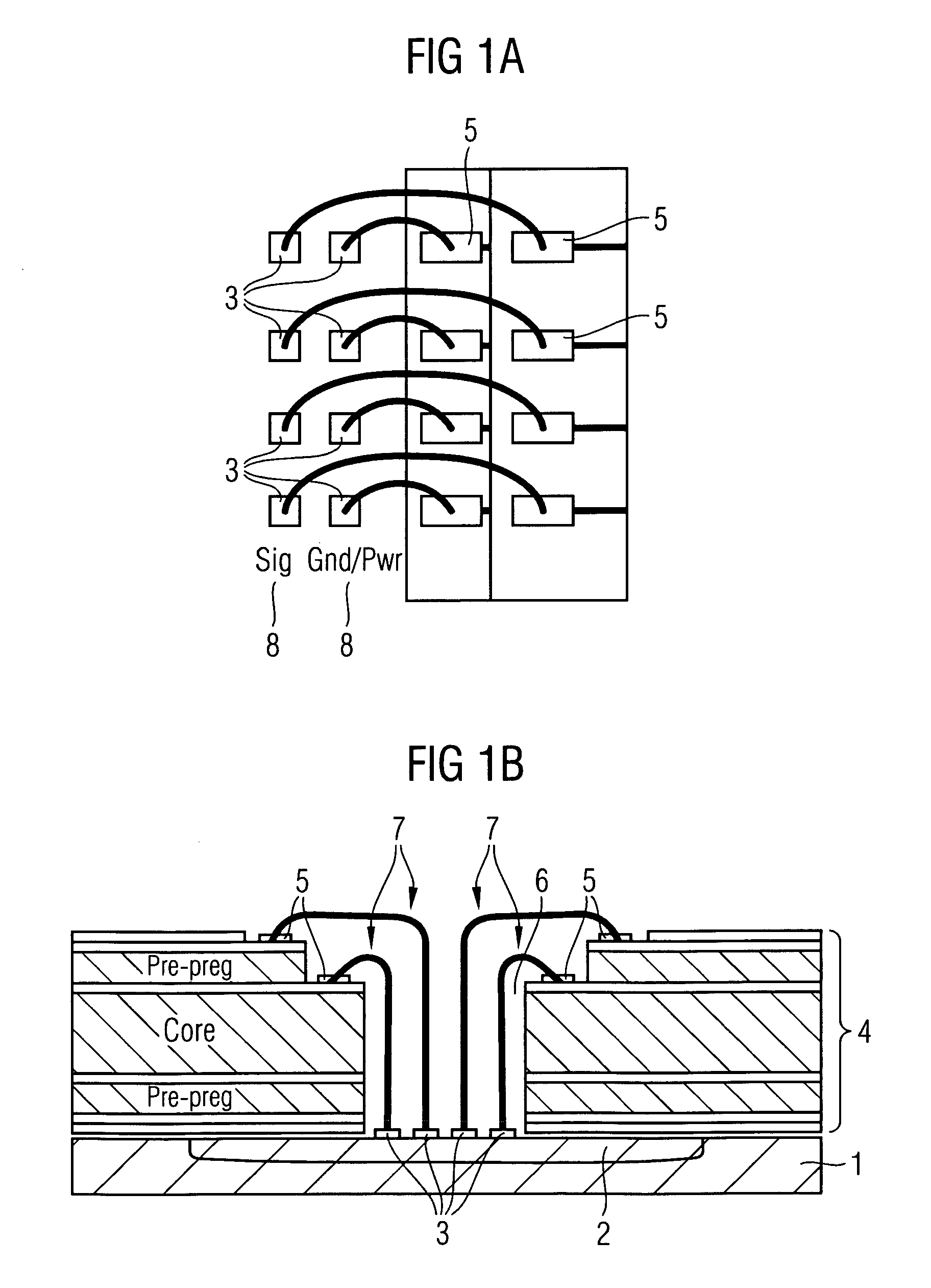
[0036]With regard to the FIGS. 1A and 1B, a section of an FBGA device is depicted. The device includes a substrate 1 in which an ...


PUM


Abstract

Embodiments provide for integrated circuit chip and device having such an integrated circuit, in which different types of pads are arranged in separate rows. In one embodiment the pads are arranged to reduce the loop inductance of corresponding signal and power supply bond wires.

Description

BACKGROUND OF THE INVENTION[0001]1. Field of the Invention[0002]The present invention refers to an integrated circuit chip having a number of pads to connect an integrated circuit. The present invention further refers to an integrated device including a packaged integrated circuit chip and interconnection means.[0003]2. Description of the Related Art[0004]The electrical performance of integrated devices increasingly develops into a limiting factor in high-speed memory packages, e.g. for graphics applications. Proper signal routing, particularly in a package, becomes more and more important for the signal quality. The signal routing comprises the signal trace and the corresponding return path through power and ground planes / traces. One of the main issues is the noise generated by the non-ideal power supply system. To reduce the noise, the inductance of the loop power supply / ground-signal-trace has to be minimized and the required line characteristic impedance has to be maintained con...

Claims


Application Information

Patent Timeline
Patent Type & Authority Patents(United States)
IPC IPC(8): H01L23/48
CPCH01L23/13H01L23/50H01L23/66H01L24/06H01L24/49H01L23/49822H01L2224/05554H01L2223/6611H01L2224/05599H01L2224/48091H01L2224/48095H01L2224/4824H01L2224/49109H01L2224/49174H01L2224/4943H01L2224/85399H01L2924/014H01L2924/14H01L2924/30107H01L2924/3011H01L2924/12041H01L2224/32225H01L2224/73215H01L2224/48227H01L2924/01033H01L2924/00014H01L24/48H01L2224/45099H01L2924/00H01L2224/49052H01L2224/49431H01L2224/49433
Inventor GOSPODINOVA, MINKATHOMAS, JOCHENSAVIGNAC, DOMINIQUE
Owner QIMONDA
Why Eureka
Try Eureka