Off-axis illumination assembly and method

a technology of off-axis illumination and assembly, which is applied in the direction of inking apparatus, circuit inspection/indentification, instruments, etc., can solve the problems of less efficient illumination of shaped solder paste deposits and difficulty in viewing using only on-axis illumination

Active Publication Date: 2008-12-02
SPEEDLINE TECH
View PDF18 Cites 13 Cited by
  • Summary
  • Abstract
  • Description
  • Claims
  • Application Information

AI Technical Summary

Problems solved by technology

Specifically, it is shown that the sloped sides and irregular top surfaces of poorly shaped solder paste deposits are less efficiently illuminated and therefore more difficult to view using only on-axis illumination only.

Method used


Image

  • Off-axis illumination assembly and method
  • Off-axis illumination assembly and method
  • Off-axis illumination assembly and method

Examples


Embodiment Construction

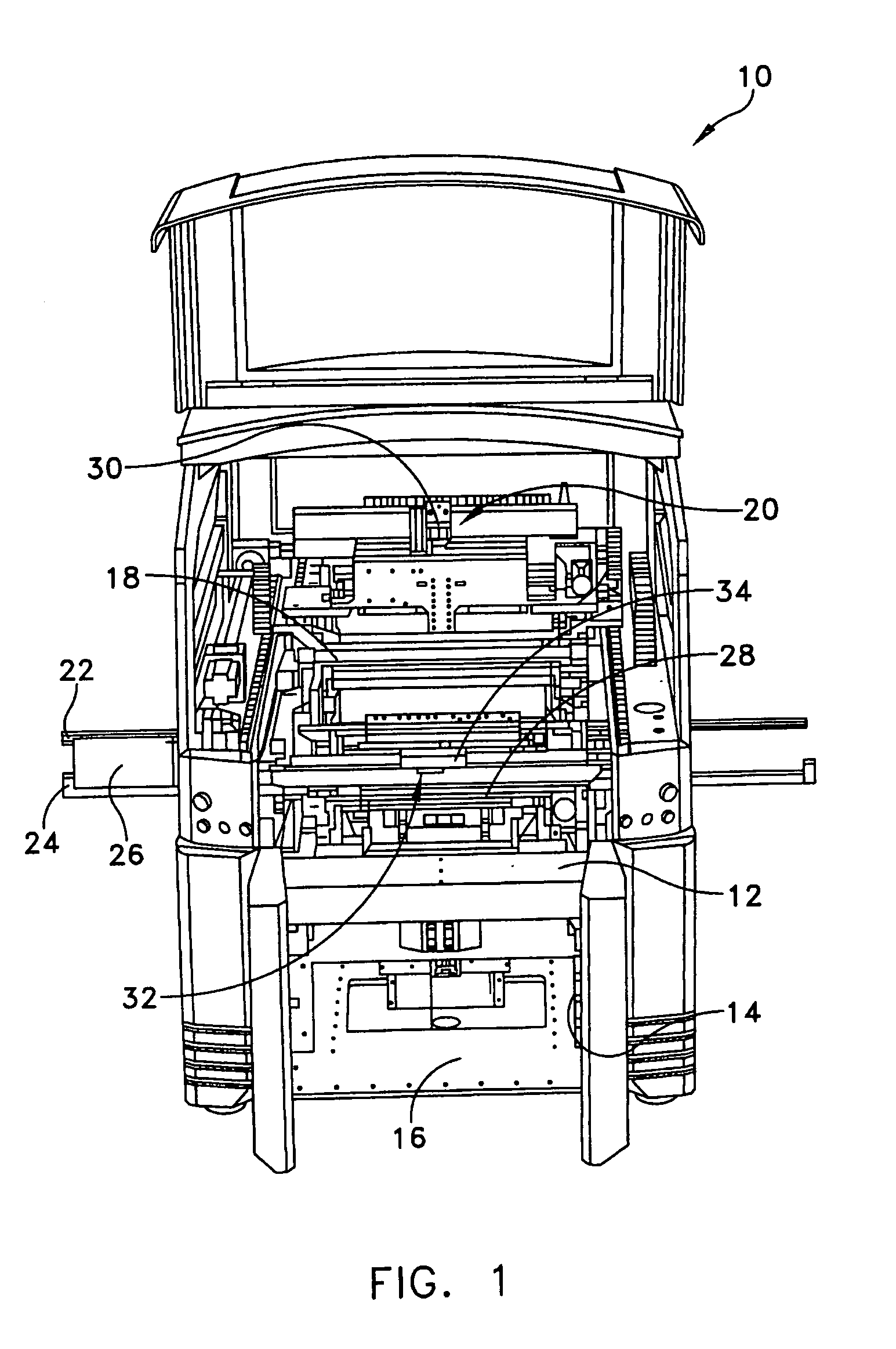
[0038]For purposes of illustration, embodiments of the present invention will now be described with reference to a stencil printer used to print solder paste onto a circuit board. One skilled in the art will appreciate that embodiments of the present invention are not limited to stencil printers that print solder paste onto circuit boards, but rather, may be used in other applications requiring dispensing of other viscous materials, such as glues, encapsulents, underfills, and other assembly materials suitable for attaching electronic components onto a circuit board. Thus, any reference to solder paste herein contemplates use of such other materials. Also, the terms “screen” and “stencil” may be used interchangeably herein to describe a device in a printer that defines a pattern to be printed onto a substrate.

[0039]FIG. 1 shows a front perspective view of a stencil printer, generally indicated at 10, in accordance with one embodiment of the present invention. The stencil printer 10 ...


PUM


Abstract

A stencil printer is provided for depositing solder paste onto a surface of an electronic substrate. The stencil printer includes a frame and a stencil coupled to the frame. The stencil has a plurality of apertures formed therein. The stencil printer further includes a dispenser coupled to the frame. The stencil and the dispenser are adapted to deposit solder paste onto the electronic substrate. The stencil printer further includes an imaging system constructed and arranged to capture an image of the electronic substrate. The imaging system includes a camera assembly, an on-axis illumination assembly adapted to generate light substantially along a first axis generally perpendicular to the surface of the electronic substrate, and an off-axis illumination assembly adapted to generate rays of light substantially along a second axis extending at an angle with respect to the first axis. A controller is coupled to the imaging system to control movement of the imaging system to capture an image.

Description

FIELD OF THE INVENTION[0001]The present invention relates to apparatuses and processes for dispensing material, and more particularly to an apparatus and process for printing solder paste through a screen or stencil printer onto an electronic substrate, such as a printed circuit board.BACKGROUND OF THE INVENTION[0002]In typical surface-mount circuit board manufacturing operations, a stencil printer is used to print solder paste onto a circuit board. Typically, a circuit board having a pattern of pads or other conductive surfaces onto which solder paste will be deposited is automatically fed into the stencil printer and one or more small holes or marks on the circuit board, called fiducials, is used to align the circuit board with a stencil or screen of the printer prior to the printing of solder paste onto the circuit board. After the circuit board is aligned, the board is raised to the stencil (or in some configurations, the stencil is lowered to the circuit board), solder paste is...

Claims


Application Information

Patent Timeline
Patent Type & Authority Patents(United States)
IPC IPC(8): B05C17/04
CPCG01N21/95684H05K3/1233B41P2215/00B41P2215/11H05K2203/163H05K1/0269G01N2021/8825G01N21/956H05K3/1216B41F15/14H05K3/12B41M1/12
Inventor PRINCE, DAVID P.
Owner SPEEDLINE TECH
Why Eureka
Try Eureka