Photomask for off-axis illumination and method of fabricating the same

a technology of off-axis illumination and photomask, which is applied in the direction of photomechanical equipment, originals for photomechanical treatment, instruments, etc., can solve the problems of limited resolution which can be achieved, practicably impossible to employ the method in mass production, and difficult to form patterns in the x and y-directions and the diagonal direction under only one illumination condition

Inactive Publication Date: 2005-03-15
SAMSUNG ELECTRONICS CO LTD
View PDF7 Cites 11 Cited by
  • Summary
  • Abstract
  • Description
  • Claims
  • Application Information

AI Technical Summary

Benefits of technology

Beneficially, the phase gratings are formed together with the photomask as one body on the back surface of the photomask, and thereby overcoming the OAI limit of the exposure equipment, and allowing OAI of an incident light sou

Problems solved by technology

However, there are limits to the resolution which can be attained.
The intensity of light is not reduced as when using the modified aperture, but problems may occur when the grating mask is attached to the back surface of the photomask.
Various losses and uncontrollable reasonable factors, such as that the grating mask must be detached and reattached for cleaning after being used for a certain time, are inherent in this method, and thus, it is practically impossible to employ the method in mass production.
However, when patterns transferred onto the wafer have pitches in an x-direction, a y-direction, and a diagonal direction, at different intervals, it is

Method used


Image

  • Photomask for off-axis illumination and method of fabricating the same
  • Photomask for off-axis illumination and method of fabricating the same
  • Photomask for off-axis illumination and method of fabricating the same

Examples


first embodiment

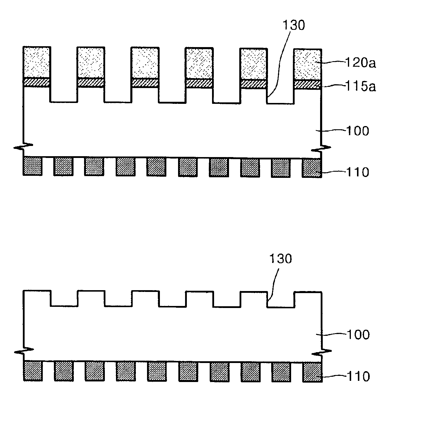
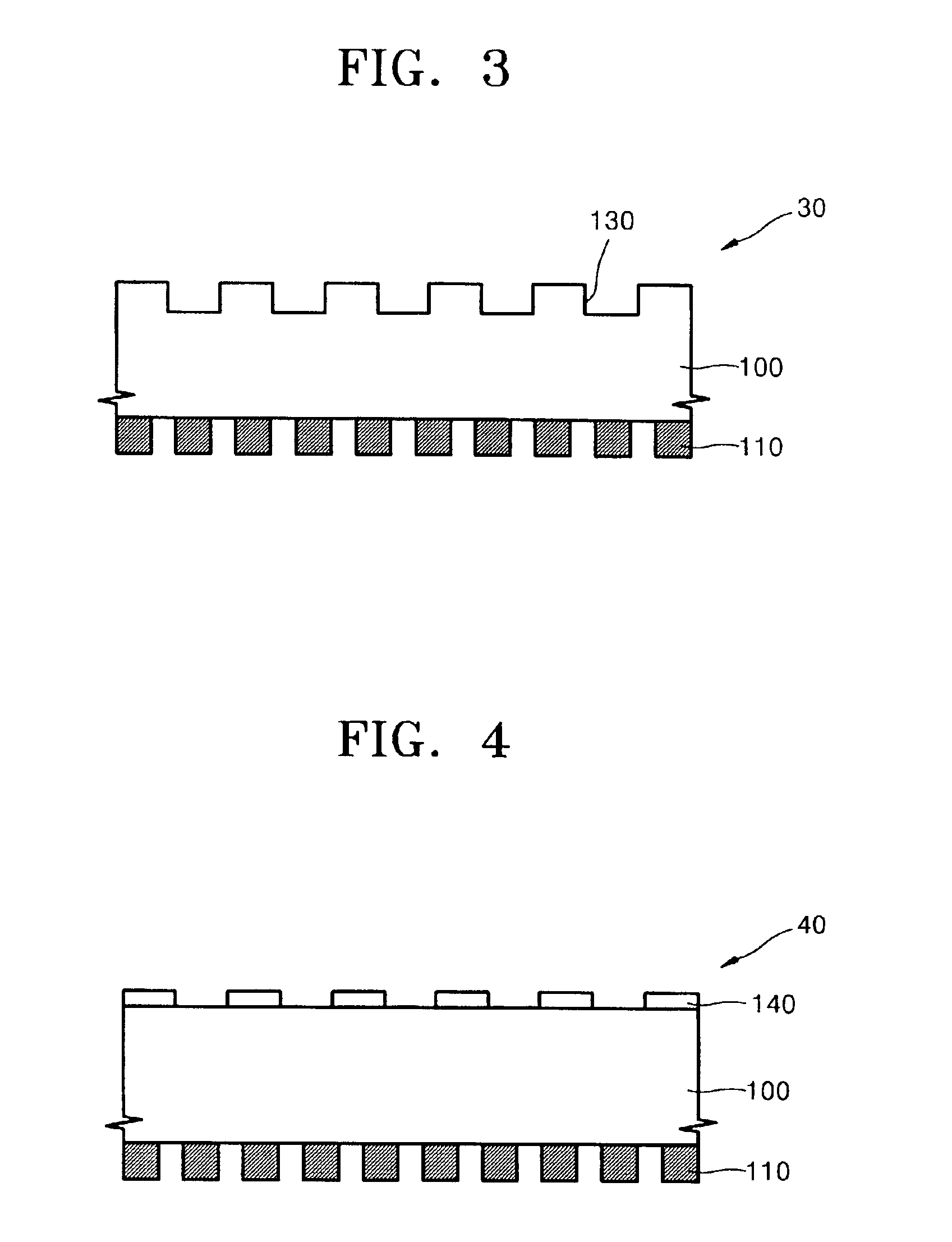
Referring to FIG. 3, a photomask 30 according to the present invention is formed on a transparent substrate 100. The transparent substrate 100 is formed of glass or quartz. A plurality of opaque patterns 110 for defining a floodlighting portion for forming patterns are formed on the front surface of the transparent substrate 100. The opaque patterns 10 may be patterns for forming a DRAM but are not limited to this. The opaque patterns 10 may be formed of a proper opaque material, for example, chrome (Cr).

A plurality of phase gratings 130 are formed on the back surface of the transparent substrate 100. As shown in FIG. 3, the plurality of phase gratings 130 have regularly periodical unevenness. Here, the phase gratings 130 are formed by etching the back surface of the transparent substrate 100.

second embodiment

Referring to FIG. 4, a photomask 40 according to the present invention includes a transparent substrate 100, a plurality of opaque patterns 10 that are formed on the front surface of the transparent substrate 100, and a plurality of phase gratings 140 that are formed on the back surface of the transparent substrate 100. The phase gratings 140 are formed together with the transparent substrate 100 as one body. Specifically, a material layer having a phase difference, such as a spin on glass (SOG) layer, is formed on the back surface of the transparent substrate 100 and then etched to form the phase gratings 140.

The phase gratings included in the photomasks 30 and 40 are formed to allow off-axis illumination (OAI) of an incident light source beyond the OAI limit of exposure equipment, to allow use in the outmost region of an aperture, and to allow modified illumination in a shape suitable for the layout of the opaque patterns. Although an arbitrary proper phase grating is used in the ...


PUM


Abstract

A photomask that is capable of implementing off-axis illumination (OAI), and a method of fabricating the same, are provided. The photomask includes a transparent substrate, a plurality of opaque patterns formed on the front surface of the transparent substrate, for defining a floodlighting portion for forming patterns, and a plurality of phase gratings formed on the back surface of the transparent substrate, allowing off-axis illumination (OAI) of an incident light source beyond the OAI limit of exposure equipment, allowing use in the outmost region of an aperture, and allowing modified illumination having a shape suitable for the layout of the opaque patterns.

Description

CROSS REFERENCES TO RELATED APPLICATIONSThis application claims priority under 35 U.S.C. §119 from Korean Patent Application No. 2002-6836, filed on 6 Feb. 2002, the contents of which are hereby incorporated by reference in their entirety as if fully set forth herein.BACKGROUND OF THE INVENTION1. Field of the InventionThe present invention relates to a photomask for fabricating a semiconductor device, and a method of fabricating the same, and more particularly, to a photomask on which phase gratings are formed for off-axis illumination (OAI), and a method of fabricating the same.2. Description of the Related ArtPhotomask images or patterns, which define various elements in a photolithographic process, are focused onto photoresist using light. In order to implement tiny features, finer images must be focused on the photoresist, and optical resolution must be increased. However, there are limits to the resolution which can be attained.Thus, in order to fabricate a semiconductor device...

Claims


Application Information

Patent Timeline
IPC IPC(8): G03F7/20G03F1/14G03F1/26G03F1/68G03F1/76G03F1/78G03F1/80H01L21/027
CPCG03F1/144G03F7/70125G03F1/34G03F1/50H01L21/027
Inventor SHIN, IN-KYUNSOHN, JUNG-MINYOON, HEE-SUNCHOI, SEONG-WOON
Owner SAMSUNG ELECTRONICS CO LTD
Why Eureka
Try Eureka