Microcontactor probe assembly having a plunger and electric probe unit using the same

a microcontactor and probe assembly technology, applied in the field of microcontactor probes, can solve the problems of reducing the service life of the substrate, reducing the accuracy of inspection, and reducing the accuracy of inspection, and achieve the effect of improving the accuracy of inspection

Inactive Publication Date: 2008-12-02
NHK SPRING CO LTD
View PDF16 Cites 8 Cited by
  • Summary
  • Abstract
  • Description
  • Claims
  • Application Information

AI Technical Summary

Benefits of technology

[0012]It therefore is an object of the present invention to provide a microcontactor probe and an electric probe unit, in which a conduction path has a reduced number of sliding portions for conduction, without increase in inductance nor resistance, thereby permitting an enhanced accuracy of inspection.
[0013]To achieve the object, according to an aspect of the present invention, there is provided a microcontactor probe comprising: an insulator formed with a support hole having an open end and a close end; a lead conductor exposed inside the support hole at the close end; and a resilient conductive assembly fitted in the support hole and kept from falling, the assembly comprising a first conductor portion exposed outside at the open end, and a second conductor portion contacting the lead conductor, wherein one of the first and second conductor portions comprises a tubular conductor portion slidably contacting at one part thereof on the other of the first and second conductor portions, and a fixed conductor portion fixed to another part of the tubular conductor portion. According to this aspect of the present invention, the tubular conductor portion which has a single sliding contact still can reduce inductance at high frequencies.

Problems solved by technology

In the microcontactor probe 100, however, the conduction path L includes, as shown in FIG. 13, lower and upper sliding portions A and B for conduction between the intermediate tight wound spiral portion 2a and the stem parts 3a and 4a of the lower and upper plungers 3 and 4, respectively, which two sliding portions A and B for conduction cause dispersion of resistance, resulting in a reduced accuracy of inspection, as a problem.
There is thus required a great contact pressure, which however is concurrently exerted via the plunger 4 also on the lead conductor 11, which means that in application to a mass production the lead conductor 11 is subjected to a great contact pressure imposed thereon every test (that amounts to hundreds of thousands to millions times), resulting in a reduced service life at the substrate 13 (or the wiring plate 10) due to an early rupture or the like, as another problem.

Method used


Image

  • Microcontactor probe assembly having a plunger and electric probe unit using the same
  • Microcontactor probe assembly having a plunger and electric probe unit using the same
  • Microcontactor probe assembly having a plunger and electric probe unit using the same

Examples


first embodiment

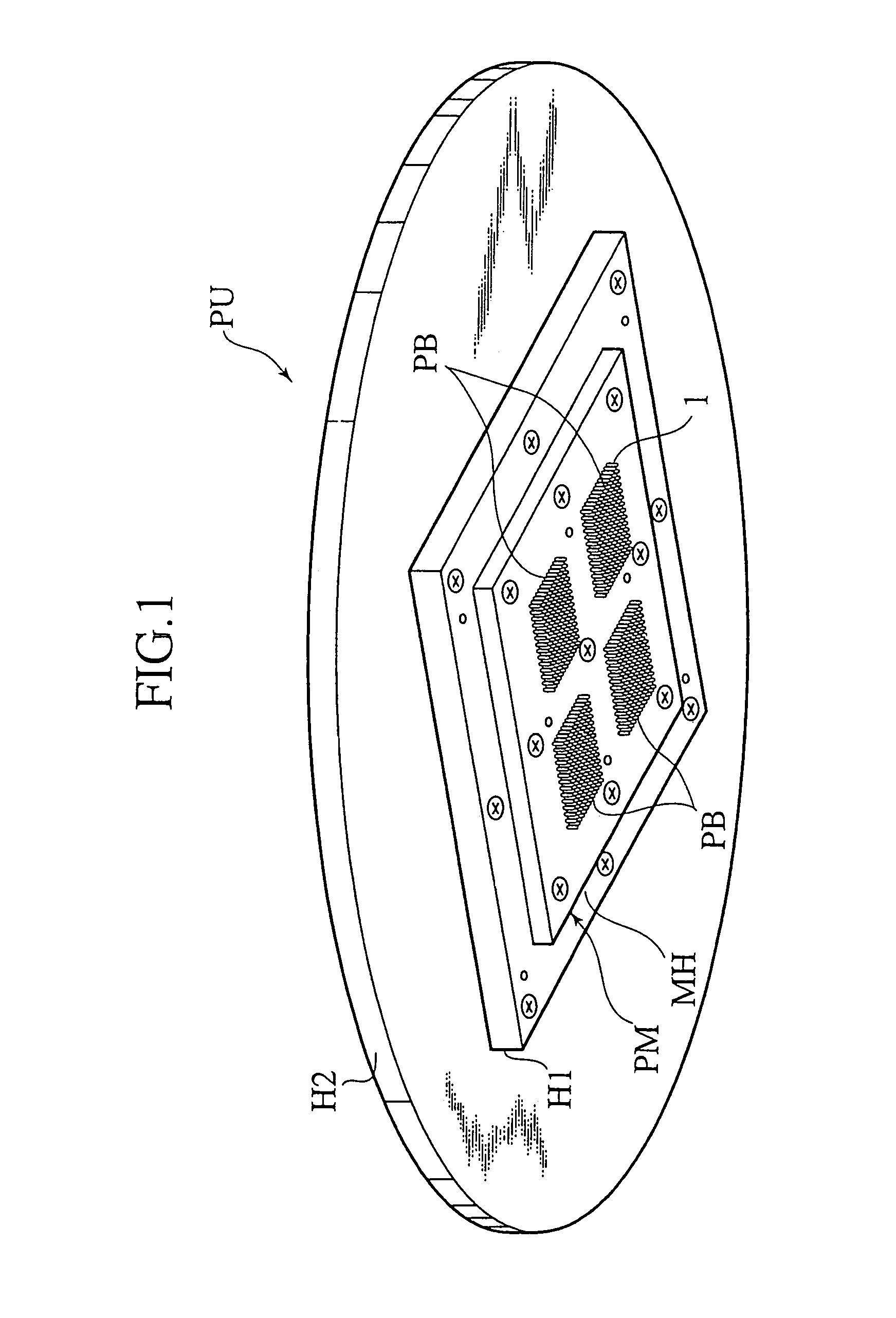
[0035]FIG. 1 shows an electric probe unit PU according to the invention. The probe unit PU is constituted as a probe card, including a both-sided performance board H2 as a relatively large substrate and a substantially flat transformer H1 as a relatively small repeating substrate fastened to a downside of the performance board H2 by screws, and with at least one electric probe module PM fastened to a downside of the transformer H1 by screws. The probe unit PU is supported by a computer-aided multi-axis positioning robot called “tester” (not shown), so that the probe module PM can be set in an arbitrary position within a designed spatial region with an optimal attitude for inspection of a target (not shown), such as a printed circuit board, a micro chip, or a semiconductor wafer, to be probed by electrical contact for acquisition or sampling of current data or signals, such as of current conduction or performance checks.

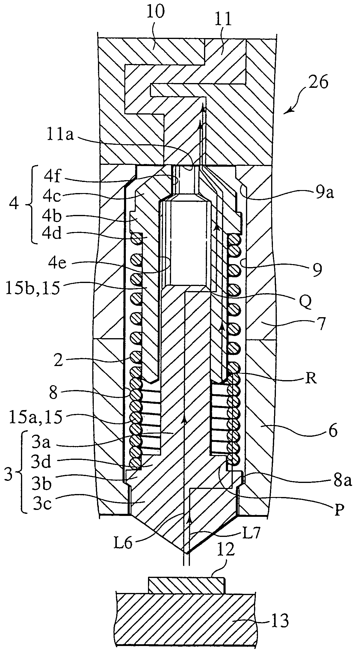
[0036]The electric probe module PM is constituted by a substanti...

second embodiment

[0054]In the second embodiment, the auxiliary spring 16 is made of a coil spring and is positioned outside of the coil spring 2 resiliently biasing the paired plungers 3 and 4, thereby to provide a coaxial double coil spring structure with the coil spring 2.

[0055]More specifically, the auxiliary spring 16 is made of a coil spring having an adequately larger diameter than the coil spring 2 and is inserted into the support hole 8 formed to have an adequately larger diameter than the support hole 9, to be extended between a bottom surface 7b of the holder 7 and the flanged part 3b formed to have an adequately larger diameter.

[0056]With the microcontactor prove 20 thus constituted, the conical tip of the needle head part 3c of the lower plunger 3 is brought into resilient contact with the target 12 of inspection formed on a substrate 13 for inspection. As shown by solid line arrows in FIG. 3, a conduction path L2 of signals in inspection extends from the target 12 through the lower plun...

third embodiment

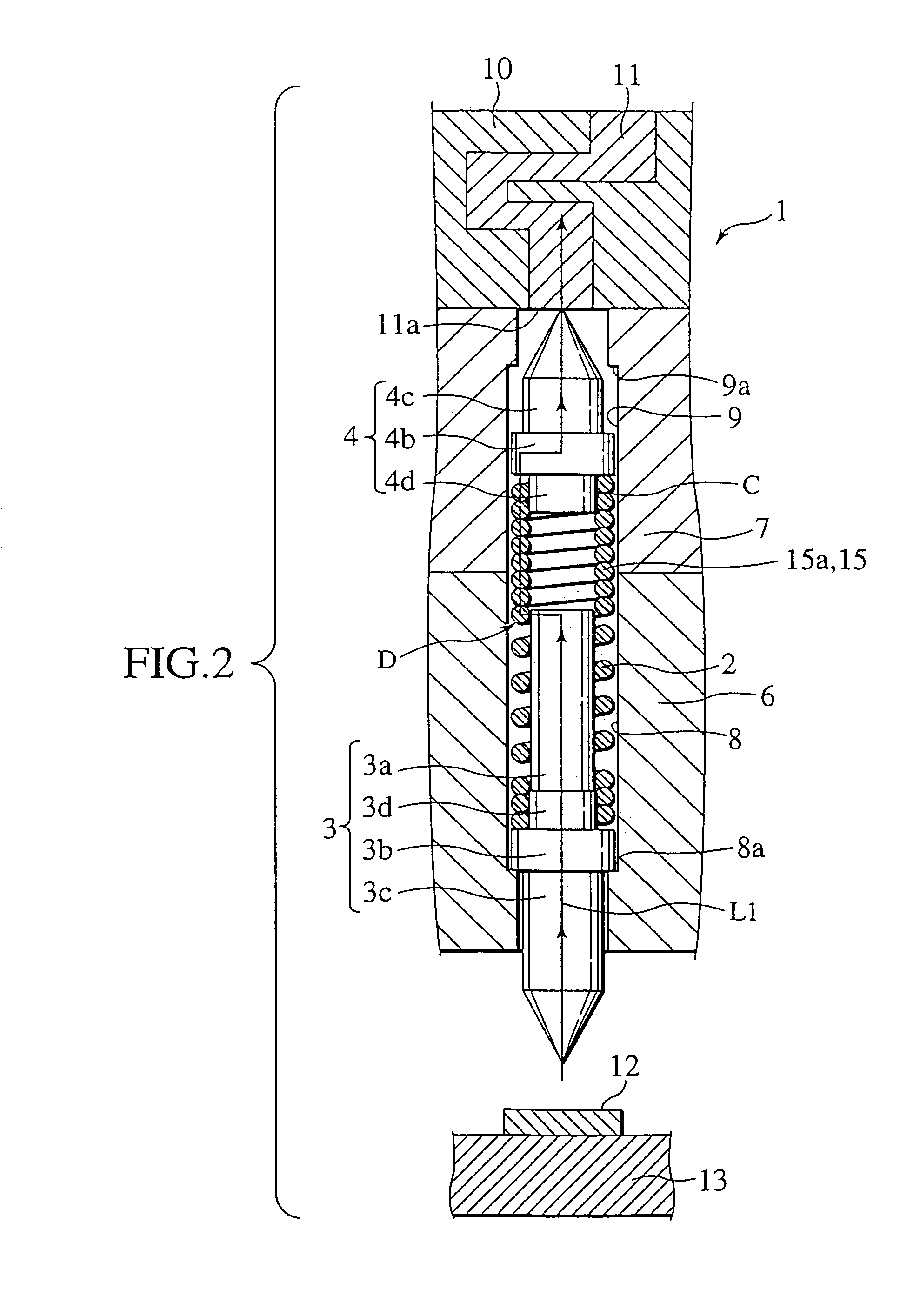
[0062]FIG. 4 shows a microcontactor probe 21 according to the present invention. The probe 21 has the same structure as that of the above-described microcontactor probe 20 except that it has a stepped flanged part 3b in a lower plunger 3.

[0063]More specifically, the flanged part 3b of the plunger 3 according to the third embodiment is constituted with a large-diameter flanged part 3e having a larger diameter than that of an auxiliary spring 16 and contacting a coil end of the auxiliary spring 16, and a small-diameter flanged part 3f integrally formed on one side of the large-diameter flanged part 3e and insertable into the coil of the auxiliary spring 16, on which part 3f a boss part 3d is formed.

[0064]Thus the microcontactor probe 21 properly has the same functional effects as those of the microcontactor probe 20 and also secures stable operation of the lower plunger 3 by mounting the plunger 3 with the small-diameter flanged part 3f inserted into the coil of the auxiliary spring 1...


PUM


Abstract

A microcontactor probe has an insulator (6, 7) formed with a support hole (8, 9) having an open end and a close end, a lead conductor (11) exposed inside the support hole (8, 9) at the close end, and a resilient conductive assembly (2, 3, 4) fitted in the support hole (8, 9) and kept from falling. The resilient conductive assembly (2, 3, 4) includes a first plunger (3) exposed outside at the open end, a second plunger (4) contacting the lead conductor (11), a tubular conductor portion (15b) on one (4) of the first and second plungers (3, 4), a stem part (3a) of the other one of the first and second plungers, at least a portion of the stem part establishing a substantially concentric relationship with the tubular conductor portion (15b) at least during a probe operation, the concentric relationship of the tubular conductor portion (15b) with the stem part (3a) minimizing resistance and induction during a probe operation, and a coil spring fitted on the first and second plungers, the coil spring (2) having a connected tight wound portion (15a) fixed to said one (4) of the first and second plungers (3, 4) at a fixed part (P) for conduction, the tight wound portion (15a) slidably contacting said other (4) of the first and second plungers (3, 4), whereby the tight wound portion (15a) minimizes resistance and induction during a probe operation.

Description

CROSS-REFERENCE TO RELATED APPLICATIONS[0001]This is a Division of U.S. patent application Ser. No. 10 / 311,096, filed Dec. 13, 2002 and published as US Publication US 2003 / 0137316, now U.S. Pat. No. 7,057,403.BACKGROUND OF THE INVENTION[0002]1. Technical Field[0003]The present invention relates to a microcontactor probe, such as an electrically conductive miniature contactor, socketpin (SCP), or thinprobe (THP), that has a plunger as a needle member adapted for contact on a contact target, such as a liquid crystal display substrate, TAB, or package substrate (PKG), to take out an electric signal to be transmitted to external circuitry via a signal transmission line, such as a lead wire. The present invention further relates to an electric probe unit constituted with a plurality of microcontactor probes.[0004]2. Background Art[0005]Conventional electric probe units for electrical inspections, such as of a printed circuit board's conductor pattern or electronic device, employ microcon...

Claims


Application Information

Patent Timeline
Patent Type & Authority Patents(United States)
IPC IPC(8): G01R31/02G01R1/067H01L21/66
CPCG01R1/06722G01R1/06772G01R1/00
Inventor KAZAMA, TOSHIO
Owner NHK SPRING CO LTD
Why Eureka
Try Eureka