
Temperature detecting semiconductor device

a technology of semiconductor devices and temperature detection, applied in the direction of pulse techniques, optical radiation measurement, instruments, etc., can solve the problems of insufficient temperature detection precision that cannot be provided in the conventional temperature detection circuit, and the inability to completely prevent the operation of erroneous devices due to temperature variation, etc., to achieve high precision

Active Publication Date: 2008-12-02
RENESAS ELECTRONICS CORP
View PDF10 Cites 8 Cited by
  • Summary
  • Abstract
  • Description
  • Claims
  • Application Information

AI Technical Summary

Benefits of technology

[0007]It is a first object of the present invention to provide a technique which is capable of detecting a temperature of a semiconductor device with high precision. In addition, it is a second object of the present invention to provide a technique which is capable of appropriately adjusting device characteristics based on a temperature detection result without being affected by a variation in manufacturing process.
[0009]The temperature signal which is varied according to the temperature of the semiconductor device is generated based on the first clock signal having the positive temperature characteristics with respect to the frequency and the second clock signal having the negative temperature characteristics with respect to the frequency. Therefore, since the temperature signal which is sensitively varied according to the temperature of the semiconductor device is capable of being generated, temperature detection precision is improved.

Problems solved by technology

However, sufficient temperature detection precision cannot be provided in the conventional temperature detection circuit, so that an erroneous operation of the device due to a temperature variation could not be completely prevented.

Method used


Image

  • Temperature detecting semiconductor device
  • Temperature detecting semiconductor device
  • Temperature detecting semiconductor device

Examples


first embodiment

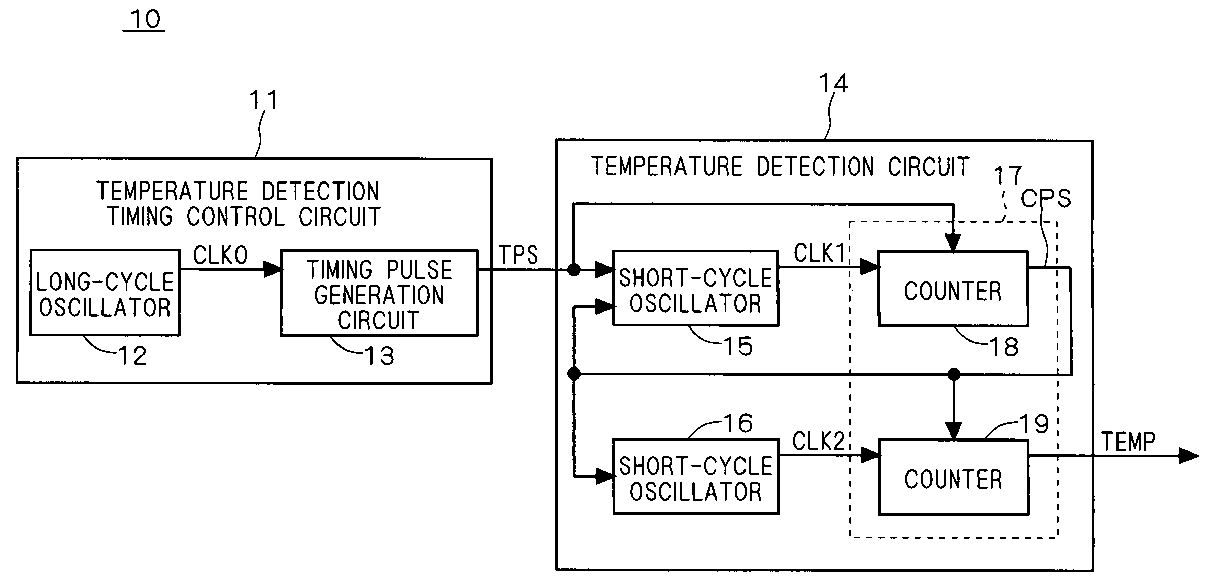
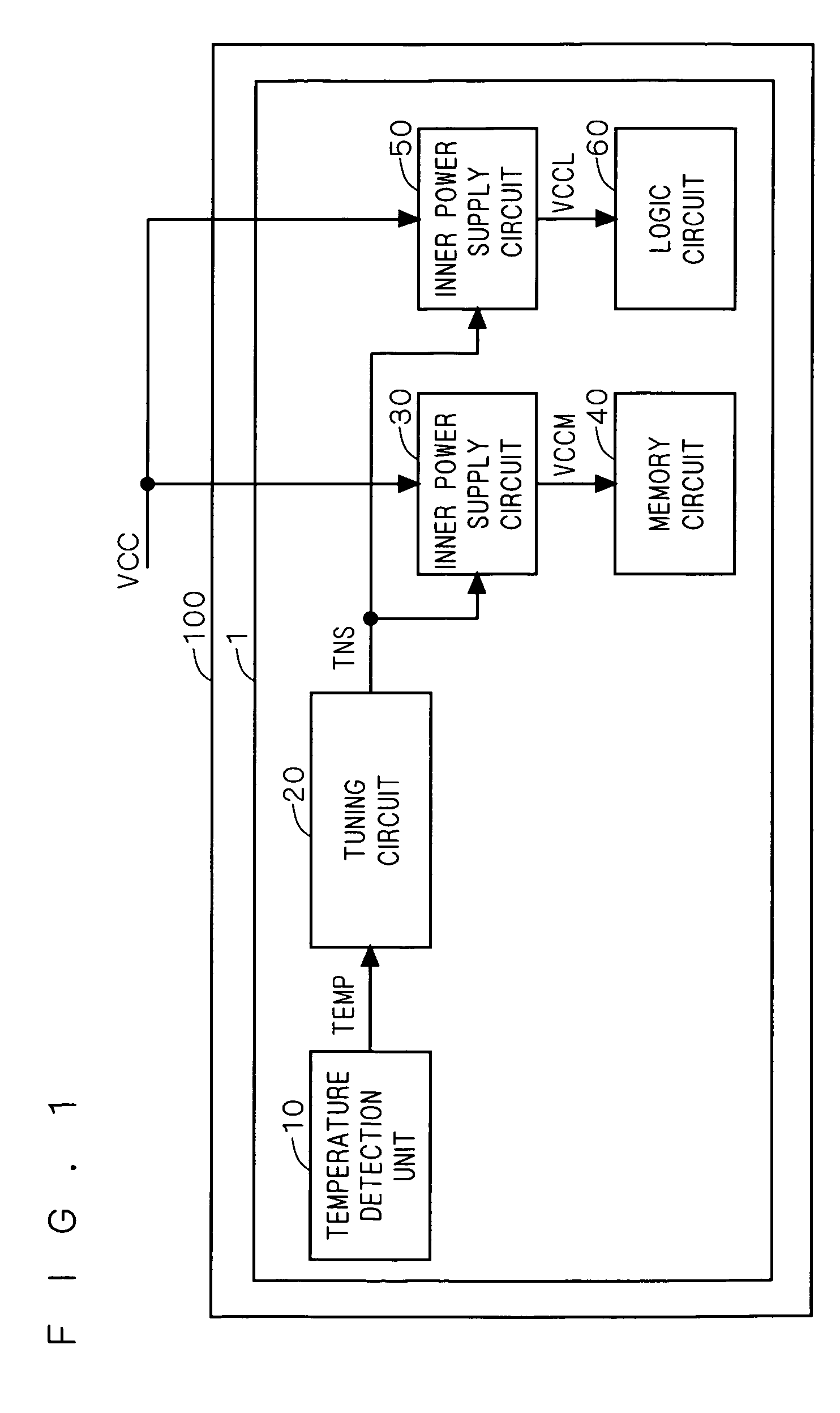
[0034]FIG. 1 is a block diagram showing a constitution of a semiconductor device according to a first embodiment of the present invention. As shown in FIG. 1, the semiconductor device according to the first embodiment includes a temperature detection unit 10, a tuning circuit 20, an inner power supply circuits 30 and 50, a memory circuit 40, and a logic circuit 60. These components are formed on a single semiconductor substrate 1 and the semiconductor substrate 1 is housed in a resin package 100.

[0035]The temperature detection unit 10 detects a temperature T of the semiconductor device, and outputs its result as a temperature signal TEMP. The tuning circuit 20 generates an adjustment signal TNS based on the temperature signal TEMP outputted from the temperature detection unit 10 and supplies the adjustment signal TNS to the inner power supply circuits 30 and 50 so as to adjust their characteristics.

[0036]The inner power supply circuit 30 is a step-down power supply circuit, for exam...

second embodiment

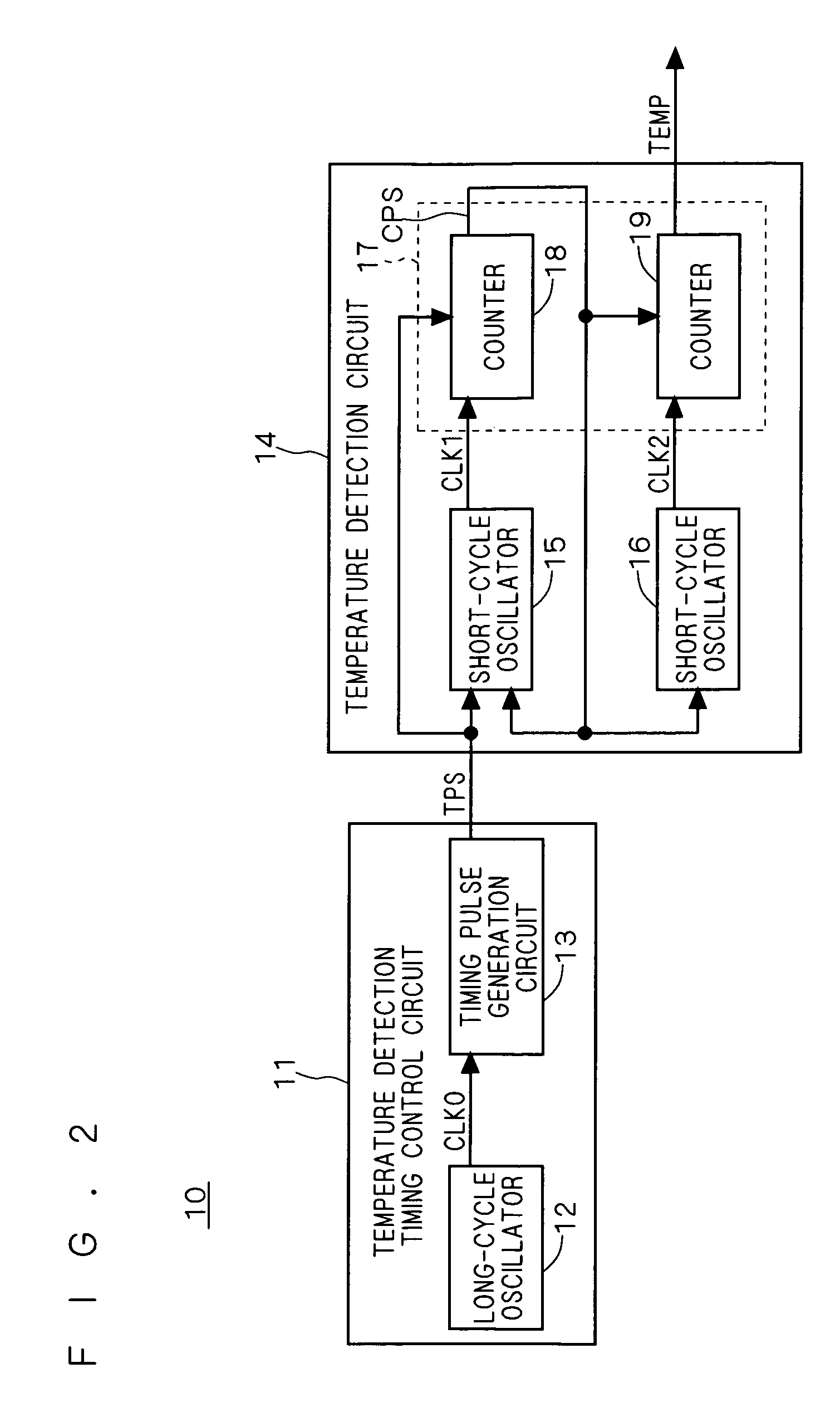
[0084]Although the number of pulses of the clock signal CLK2 counted while the clock signal CLK1 is counted by N is outputted as the temperature signal TEMP in the semiconductor device according to the first embodiment, the number of pulses of the clock signals CLK1 and CLK2 may be counted for a predetermined period of time and a difference between the counted numbers may be outputted as the temperature signal TEMP. A description will be made of a detection circuit of a temperature T in this case hereinafter.

[0085]FIG. 13 is a block diagram showing a constitution of a temperature detection circuit 74 according to a second embodiment of the present invention. The temperature detection circuit 74 according to the second embodiment is used instead of the temperature detection circuit 14 in the semiconductor device according to the first embodiment.

[0086]As shown in FIG. 13, the temperature detection circuit 74 includes the above-described short-cycle oscillators 15 and 16 and a tempera...

third embodiment

[0095]Although the inner power supply circuits 30 and 50 are provided as the circuits whose characteristics are adjusted by the tuning circuit 20 in the first embodiment, the characteristics of the circuit other than the inner power supply circuits 30 and 50 can be adjusted by using the temperature signal TEMP of the present invention. According to a third embodiment, an example of the circuit other than the circuit to be adjusted will be described.

[0096]FIG. 15 is a block diagram showing a constitution of a timing generation circuit 90 whose electrical characteristics can be adjusted according to the temperature T by the above temperature detection circuit 10 and the tuning circuit 20. In an asynchronous circuit such as a DRAM, a plurality of timing pulse signals having different rising timings from each other are needed in general. The timing generation circuit 90 generates a plurality of timing pulse signals TPS1 to TPS5 to be supplied to the asynchronous circuit. For example, th...


PUM

PropertyMeasurementUnit
temperatureaaaaaaaaaa
frequencyaaaaaaaaaa
timeaaaaaaaaaa

Abstract

There is provided a technique which is capable of detecting a temperature of a semiconductor device with high precision. A temperature detection circuit detecting a temperature of a semiconductor device includes a first short-cycle oscillator generating a first clock signal having positive temperature characteristics with respect to a frequency, a second short-cycle oscillator generating a second clock signal having negative temperature characteristics with respect to the frequency, and a temperature signal generation unit generating a temperature signal which is varied according to the temperature of the semiconductor device based on the first and second clock signals.

Description

BACKGROUND OF THE INVENTION[0001]1. Field of the Invention[0002]The present invention relates to a semiconductor device having a temperature detection function.[0003]2. Description of the Background Art[0004]Recently, semiconductor technology is miniaturized in order to implement further high speed and high integration of a semiconductor integrated circuit. Accordingly, an effect that a temperature variation has on device characteristics becomes apparent, and it is necessary to appropriately control the characteristics according to the temperature so that the device may not be erroneously operated by the temperature variation. Thus, it is necessary to correctly detect a temperature of the device, and various kinds of temperature detection circuits have been proposed conventionally. For example, Japanese Patent Application Laid-Open Nos. 2000-55742, 58-35431 (1983), 05-307882 (1993), 09-223395 (1997), 2000-269417 and 10-239097 (1998) disclose a temperature detection circuit which det...

Claims


Application Information

Patent Timeline
Patent Type & Authority Patents(United States)
IPC IPC(8): G01K7/00
CPCG01K7/01
Inventor GYOTEN, TAKAYUKIMORISHITA, FUKASHIDOSAKA, KATSUMI
Owner RENESAS ELECTRONICS CORP
Learn More