Semiconductor device
a technology of semiconductors and sublayers, applied in the direction of semiconductor devices, electrical devices, transistors, etc., can solve the problems of insufficient reduction of vk, and achieve the effect of preventing the increase of voff with a decrease in the thickness of the graded sublayer disposed between the emitter layer and the base layer
- Summary
- Abstract
- Description
- Claims
- Application Information
AI Technical Summary
Benefits of technology
Problems solved by technology
Method used
Image
Examples
first embodiment
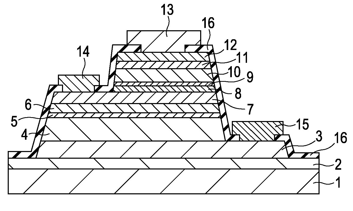
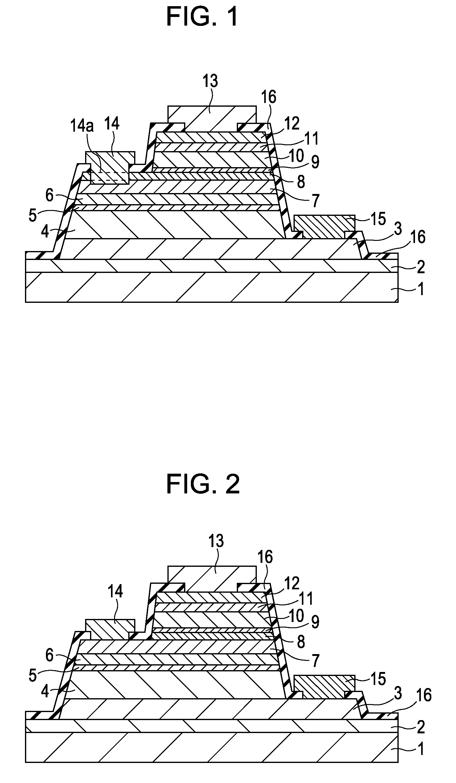
[0073]FIGS. 1 and 2 are each a cross-sectional view of a double-heterojunction HBT according to a first embodiment.
[0074]For example, a buffer layer 2, a subcollector layer 3 composed of n+-type InGaAs, a first collector sublayer 4 (hole-blocking sublayer) composed of n−-type InP, a heavily doped thin sublayer 5 composed of n+-type InP, a graded sublayer 6 composed of n−-type AlInGaAs or the like, a base layer 7 composed of p+-type InGaAs, a graded sublayer 8 composed of n−-type AlInGaAs or the like and having a thickness of about 10 nm, a heavily doped thin sublayer 9 composed of n+-type InP, a first emitter sublayer 10 (hole-blocking sublayer) composed of n−-type InP, a second emitter sublayer 11 composed of n+-type InP, and an emitter cap sublayer 12 composed of n+-type InGaAs are disposed in that order on a semi-insulating semiconductor substrate 1 composed of InP. Furthermore, the surface is covered with an insulating film 16 composed of Si3N4 or the like, except for portions f...
second embodiment
[0095]FIG. 15 is a cross-sectional view of a double-heterojunction bipolar transistor according to a second embodiment.
[0096]For example, a subcollector layer 19 composed of n+-type GaAs, a second collector sublayer 20 composed of n−-type GaAs, a first collector sublayer 21 (hole-blocking sublayer) composed of n−-type AlGaAs, a heavily doped thin sublayer 22 composed of n+-type AlGaAs, a graded sublayer 23 composed of n−-type AlGaAs or the like, a base layer 24 composed of p+-type GaAs, a graded sublayer 25 composed of n−-type AlGaAs or the like and having a thickness of about 10 nm, a heavily doped thin sublayer 26 composed of n+-type InGaP, a first emitter sublayer 27 (hole-blocking sublayer) composed of n−-type InGaP, a second emitter sublayer 28 composed of n−-type AlGaAs, a third emitter sublayer 29 composed of n+-type GaAs, and an emitter cap sublayer 30 composed of n+-type InGaAs are laminated in that order on a semi-insulating GaAs semiconductor substrate 17.
[0097]The emitte...
third embodiment
[0108]FIG. 17 is a cross-sectional view of a double-heterojunction bipolar transistor according to a third embodiment.
[0109]In this embodiment, the double-heterojunction bipolar transistor is disposed on a GaAs substrate, is mainly composed of GaAs, and includes a base layer having electron affinity greater than that of GaAs. For example, a subcollector layer 33 composed of n+-type GaAs, a collector layer 34 composed of n−-type GaAs, a heavily doped thin sublayer 36 composed of n+-type GaAs, a graded sublayer 37 composed of n−-type InGaAs or the like, a base layer 38 composed of p+-type InGaAs, a graded sublayer 39 composed of n−-type AlInGaAs or the like and having a thickness of about 10 nm, a heavily doped thin sublayer 40 composed of n+-type InGaP, a first emitter sublayer 41 composed of n−-type InGaP, a second emitter sublayer 42 composed of n-type GaAs, and an emitter cap sublayer 43 composed of n+-type InGaAs are laminated in that order on a semi-insulating GaAs semiconductor...
PUM
 Abstract
Description
Claims
Application Information


