Transmit/receive switch device

Inactive Publication Date: 2008-12-23
MARVELL INT LTD
View PDF6 Cites 147 Cited by
  • Summary
  • Abstract
  • Description
  • Claims
  • Application Information

AI Technical Summary

Benefits of technology

[0017]In still another embodiment, a communication device includes a transmitter having an output, and a power amplifier having an input coupled to the output of the transmitter, and having an output. Also, the communication device includes a low noise amplifier having an input and an output, and a receiver having an input coupled to the output of the low noise amplifier. Additionally, the communication device includes an antenna, and a transmit/receive switch having a first port coupled to the input of the low noise amplifier, a second port coupled to the output of the power amplifier, and a third port coupled to the antenna. The transmit/receive switch comprises a substrate, a receive path between the third port and the first port, and a transmit path between the third port and the second port. The transmit path includes a first transistor on the substrate, the first transistor coupled in series between the third port and the second port, wherein a body node of the first transistor is unconnected, and wherein the substrate is configured to provide a high impedance path from the first transistor to a reference voltage. The transmit/receive switch also comprises a second transistor on the substrate, the second transistor coupled in series between the first port and the reference voltage.
[0018]In yet another embodiment, another communication device includes a transmitter having an output, and a power amplifier having an input coupled to the output of the transmitter, and having an output. The communication device additionally includes a low noise amplifier having an input and an output, and a receiver having an input coupled to the output of the low noise amplifier. Further, the communication device includes an antenna, and a transmit/receive switch having a first port coupled to the input of the low noise amplifier, a second port coupled to the output of the power amplifier, and a third port coupled to the antenna. The transmit/receive switch comprises a substrate, a receive path between the third port and

Problems solved by technology

In addition to a potentially significant increase in the cost of manufacturing, the use of such external RF switches has several other drawbacks.
For example, isolation of the receiver path from the transmission path is often less than optimal, which leads to a degradation in transmission power.
Additionally, using switches external to the transceiver IC(s) increases insertion loss and non-linearity, which in turn lead to a loss of sensitivity.
Previous attempts to integrate the RF switches onto an IC were not successful in meeting performance specifications necessary in most wireless applications.
For example, many CMOS RF switch implementations are not able to meet linearity requirements at typical transmitter power levels.
This causes the receiver path to p

Method used


Image

  • Transmit/receive switch device
  • Transmit/receive switch device
  • Transmit/receive switch device

Examples


Embodiment Construction

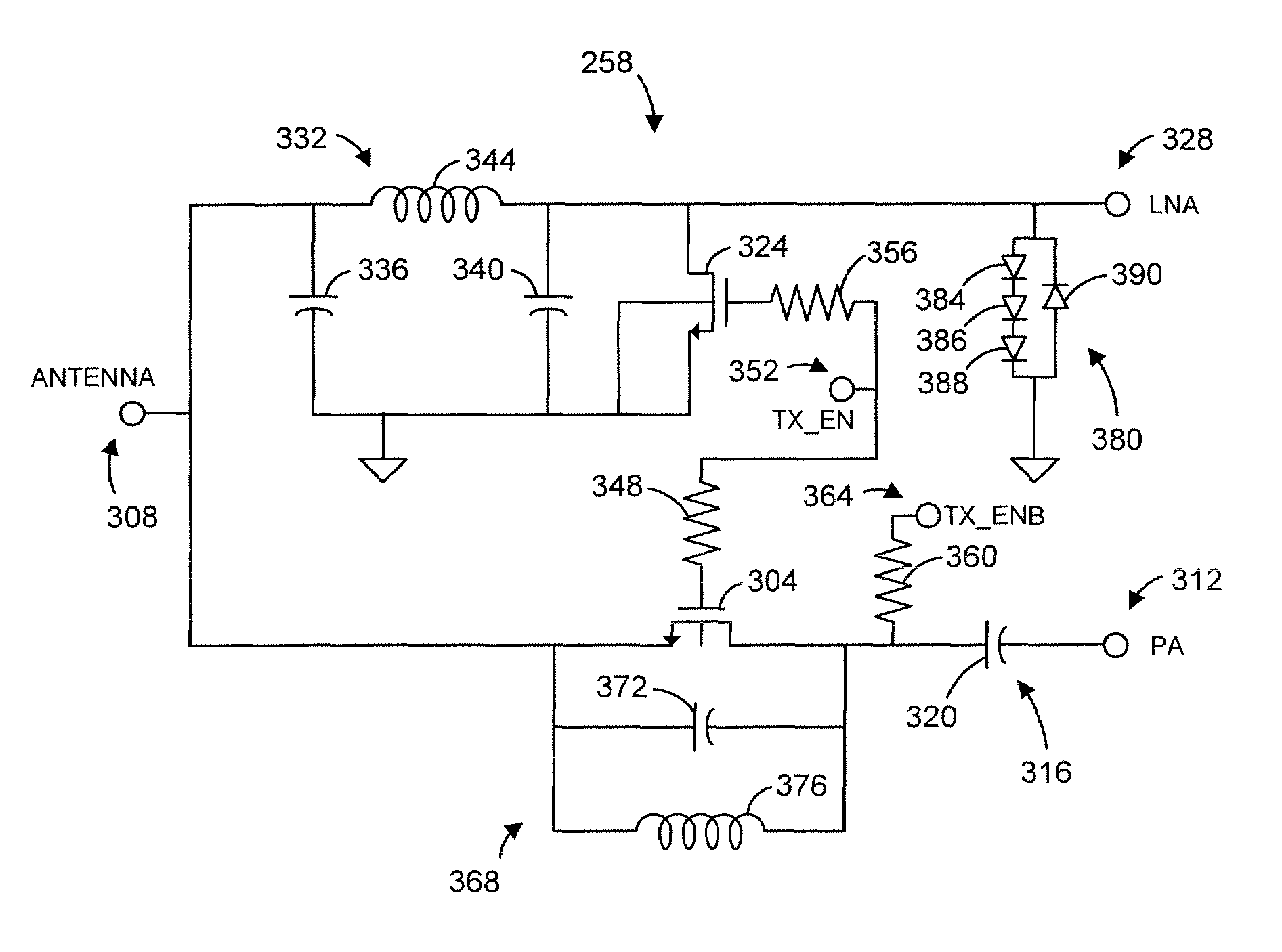
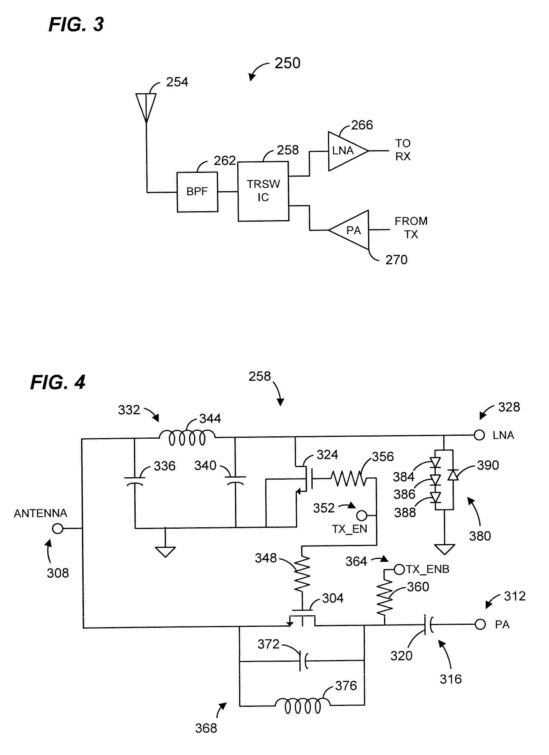
[0034]FIG. 3 is a block diagram of an example front end 250 of a transceiver that may utilize an example transmit / receive (T / R) switch to be described in more detail below. The front end 250 can be utilized in a variety of wireless communication devices such as wireless network cards, wireless access points, wireless routers, cellular telephones, personal digital assistants (PDAs) having wireless communication capability, etc. The front end 250 may include an antenna 254 coupled to a T / R switch device 258 via a band pass filter 262. As described above, the T / R switch device 258 may be implemented using standard CMOS fabrication techniques, and thus may be implemented as an integrated circuit (IC). The T / R switch device 258 may be coupled to an input of a low noise amplifier (LNA) 266 and may be coupled to an output of a power amplifier (PA) 270. During transmission, the T / R switch device 258 may couple the PA 270 to the antenna 254. Additionally, the T / R switch device 258 may isolat...


PUM


Abstract

An integrated transmit/receive (T/R) switch device comprises a substrate, an antenna port to couple with an antenna, a transmitter port to couple with a transmitter, and a receiver port to couple with a receiver. A receive path is provided between the antenna port and the receiver port, and a transmit path is provided between the antenna port and the transmitter port. The transmit path includes a first transistor on the substrate, and the first transistor is coupled in series between the antenna port and the transmitter port. A body node of the first transistor is unconnected, and the substrate is configured to provide a high impedance path from the first transistor to a reference voltage. A second transistor on the substrate is coupled in series between the receiver port and the reference voltage.

Description

CROSS-REFERENCE TO RELATED APPLICATION[0001]The present application claims the benefit of U.S. Provisional Application No. 60 / 815,361, entitled “BAZA TRANSMITTER AND RECEIVER SWITCH,” filed on Jun. 20, 2006, which is hereby incorporated by reference herein in its entirety.FIELD OF TECHNOLOGY[0002]The present disclosure relates generally to wireless communication systems and, more particularly, to radio frequency switch circuits that enable the sharing of a single antenna among transmitter and receiver stages.DESCRIPTION OF THE RELATED ART[0003]In many wireless communication devices, a single antenna is used for both transmission and reception. In some of these devices, the antenna is time shared (e.g., time-division multiplexed) between the transmitter and the receiver (transceiver). Often, radio frequency (RF) switches are used to isolate the transmission path from the receiver path so that the device is not damaged. FIG. 1 is a block diagram of an example prior art front end 100 o...

Claims


Application Information

Patent Timeline
IPC IPC(8): H03B5/00
CPCH04B1/48
Inventor TSAI, KING CHUNYAO, WEIJUNSHIN, DONG HUN
Owner MARVELL INT LTD
Why Eureka
Try Eureka