Optimized circuits for three dimensional packaging and methods of manufacture therefore

Active Publication Date: 2008-12-30
NXP USA INC
View PDF33 Cites 3 Cited by
  • Summary
  • Abstract
  • Description
  • Claims
  • Application Information

AI Technical Summary

Benefits of technology

[0004]An embodiment of the present invention provides an apparatus, comprising an integrated circuit, wherein a first portion of the integrated circuit may be placed on a first substrate and a second portion of the integrated circuit may be placed on a second substrate stacked adjacent the first substrate and wherein the first portion and the second portion of the integrated circuit may be interconnected. The first substrate may be comprised of low dielectric material and the distance between the first and the second substrate may be sufficiently large to facilitate high impedance functions and components. In an embodiment of the present invention, the integrated circuit may further comprise printing inductors on the first substrate thereby enabling them to be high Q inductors and printed spiral arms may be stacked vertically on both the top and bottom surface of the first substrate thereby creating high Q inductors.

Problems solved by technology

Often circuitry, in particular, but not limited to, wireless circuitry, occupies relatively large and expensive real estate on a module board.

Method used


Image

  • Optimized circuits for three dimensional packaging and methods of manufacture therefore
  • Optimized circuits for three dimensional packaging and methods of manufacture therefore
  • Optimized circuits for three dimensional packaging and methods of manufacture therefore

Examples


Embodiment Construction

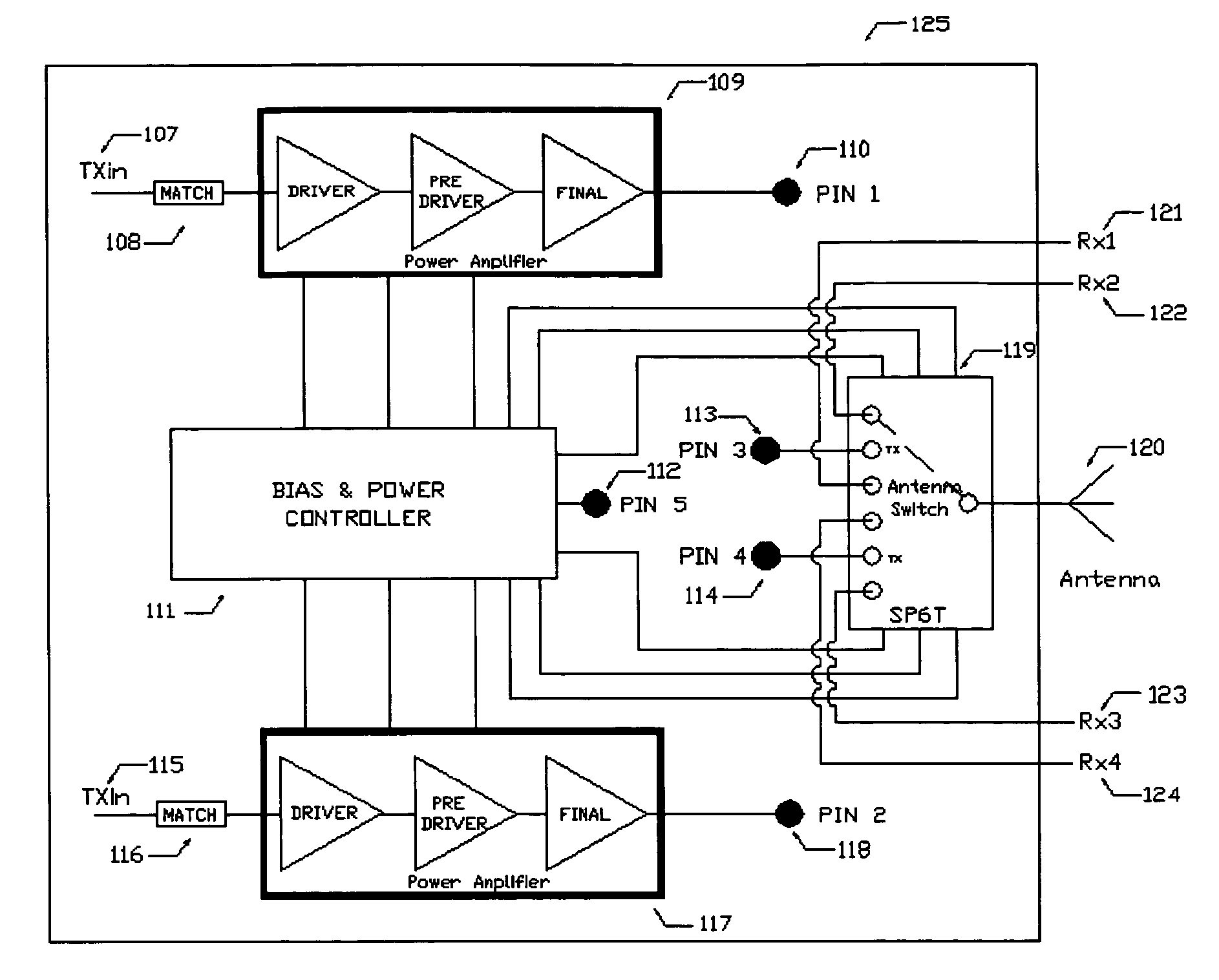
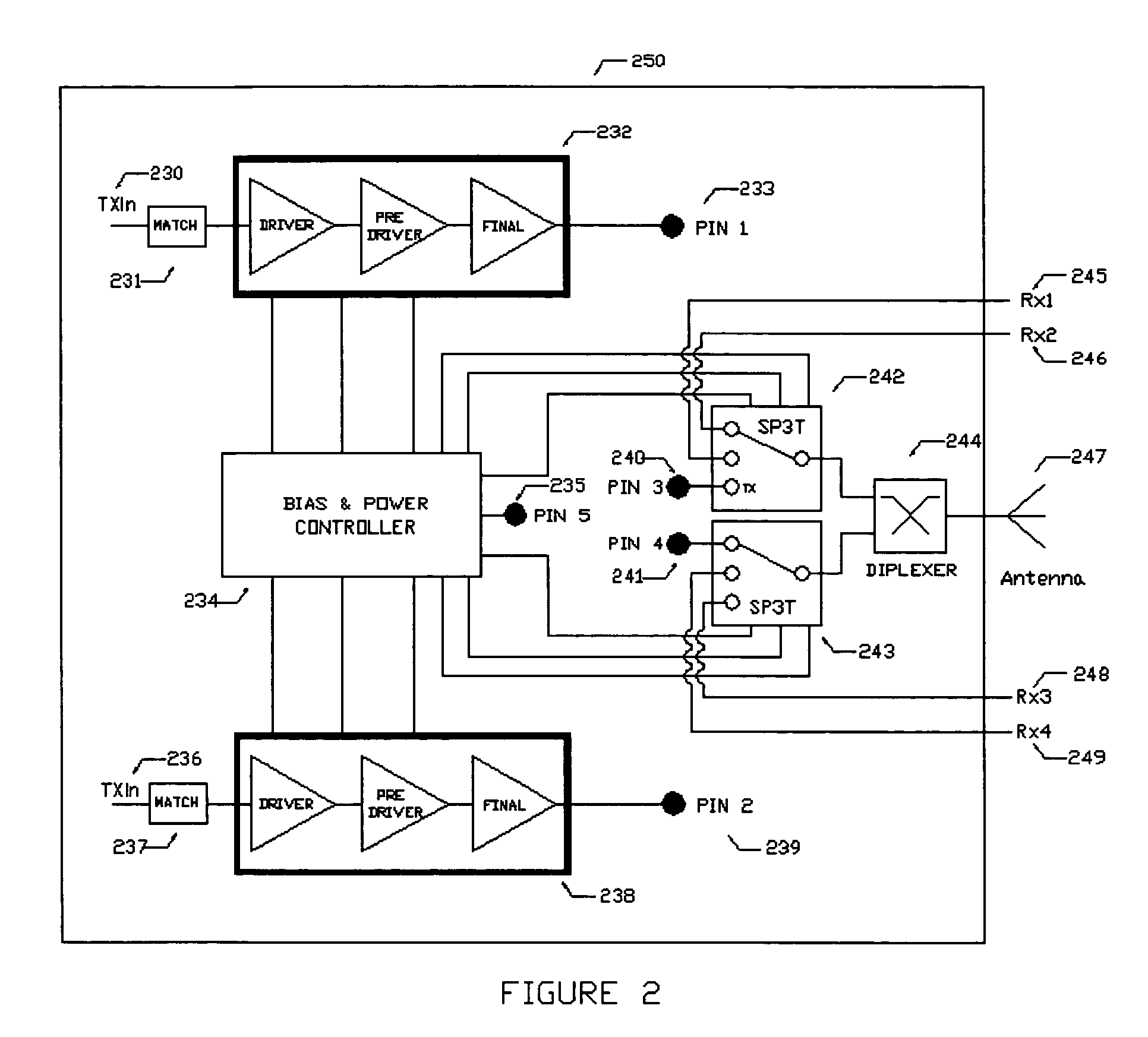
[0011]Although the present invention is not limited to only RF circuits, current design approaches for RF circuits designed for markets such as wireless products all use a single substrate onto which all components and traces are placed on. Although the substrates may have multi-layers of conductors, there is only one layer available to place components during the creation of a multi-chip module (MCM). This not only limits the size reduction, but RF performance is limited due to the sharing of one common substrate. Some components and functions work best on high impedance substrates that are thick, low dielectric constant and low loss. Other components prefer low impedance substrates that are thin and high dielectric.

[0012]Further, on conventional 2D package designs, it is extremely difficult to print high Q inductors. In an embodiment of the present invention, the multiple levels of the present 3D approach allows the construction of inductors with spirals above each other in a stac...


PUM


Abstract

An embodiment of the present invention provides an apparatus, comprising an integrated circuit, wherein a first portion of the integrated circuit is placed on a top tier substrate and a second portion of the integrated circuit is placed on a bottom tier substrate stacked adjacent the top tier substrate and wherein the first portion and the second portion of the integrated circuit are interconnected; and printed spiral arms stacked vertically on both the top and bottom surface of the top tier substrate thereby creating high Q inductors.

Description

CROSS-REFERENCE TO RELATED APPLICATION[0001]This application claims the benefit of priority under 35 U.S.C Section 119 from U.S. Provisional Application Ser. No. 60 / 653,162, filed Feb. 15, 2005, entitled, “Wireless RF Circuitry Optimized for 3D Packaging Technologies.”BACKGROUND OF THE INVENTION[0002]Packaging technology for Power Amplifier modules and Front Ends, particularly those employed in modern wireless communication networks, is moving towards a more compact and low cost packaging technology, and hence wireless circuitry must be modified and designed around the strengths of this technology.[0003]Often circuitry, in particular, but not limited to, wireless circuitry, occupies relatively large and expensive real estate on a module board. Thus, there is a strong for technologies with improved designs which can reduce the size and thus the cost of these module boards.SUMMARY OF THE INVENTION[0004]An embodiment of the present invention provides an apparatus, comprising an integra...

Claims


Application Information

Patent Timeline
IPC IPC(8): H03G3/00H03G3/20
CPCH05K1/024H05K1/142H05K1/165H05K2201/0187H05K2201/09972
Inventor MACROPOULOS, WILLIAMMENDOLIA, GREGOAKES, JAMES G.KHAYO, IZZ
Owner NXP USA INC
Why Eureka
Try Eureka