Triplate planar slot antenna

a planar slot and antenna technology, applied in the direction of resonant antennas, particular array feeding systems, radiating element structural forms, etc., can solve the problems of disadvantageous increase, disadvantageous increase, and detrimental increase of dielectric loss, so as to achieve disadvantageous increase in antenna efficiency and low gain

Active Publication Date: 2008-12-30
JAPAN RADIO CO LTD
View PDF16 Cites 2 Cited by
  • Summary
  • Abstract
  • Description
  • Claims
  • Application Information

AI Technical Summary

Benefits of technology

[0010]Generally, a planar antenna using a dielectric substrate has a larger dielectric loss at higher working frequencies. This results in the planar antenna having a significantly lower gain. In view of its lower gain, if the planar antenna is adapted to serve as a high gain antenna, the size thereof must become larger, however in this case, the antenna efficiency may become disadvantageously lower.
[0015]The present invention was made to solve the above problems, wherein an object of the present invention is to provide a high-efficiency triplate planar slot antenna in which the dielectric loss of the dielectric film, from which copper foil pieces have been removed, can be made small even if the antenna size is large.
[0016]Further, another object of the present invention is to provide a triplate planar slot antenna in which characteristic variations between antennas can be prevented, even if the working frequency range is wide.Means For Solving The Problems

Problems solved by technology

In view of its lower gain, if the planar antenna is adapted to serve as a high gain antenna, the size thereof must become larger, however in this case, the antenna efficiency may become disadvantageously lower.
Thus, the dielectric loss may detrimentally increase.
Since the thickness thereof is substantially 50 μm at a minimum, the dielectric loss may disadvantageously increase.

Method used


Image

  • Triplate planar slot antenna
  • Triplate planar slot antenna
  • Triplate planar slot antenna

Examples


Embodiment Construction

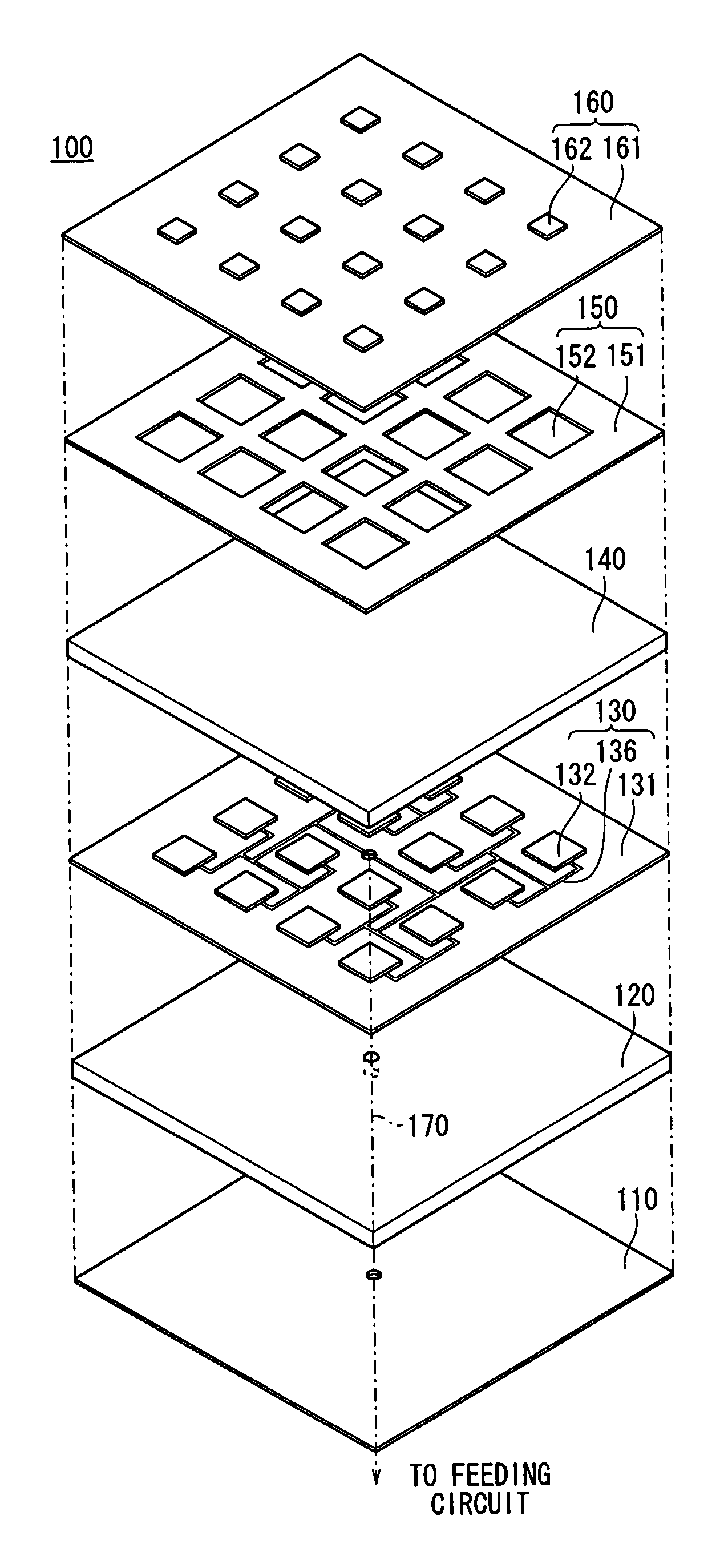
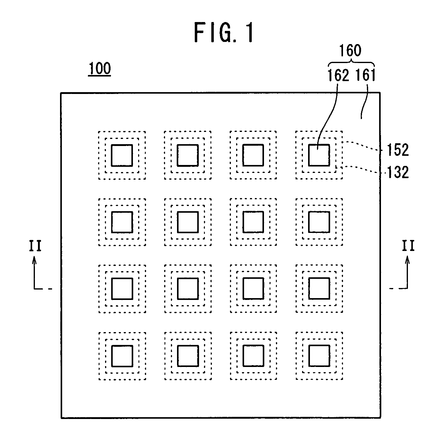
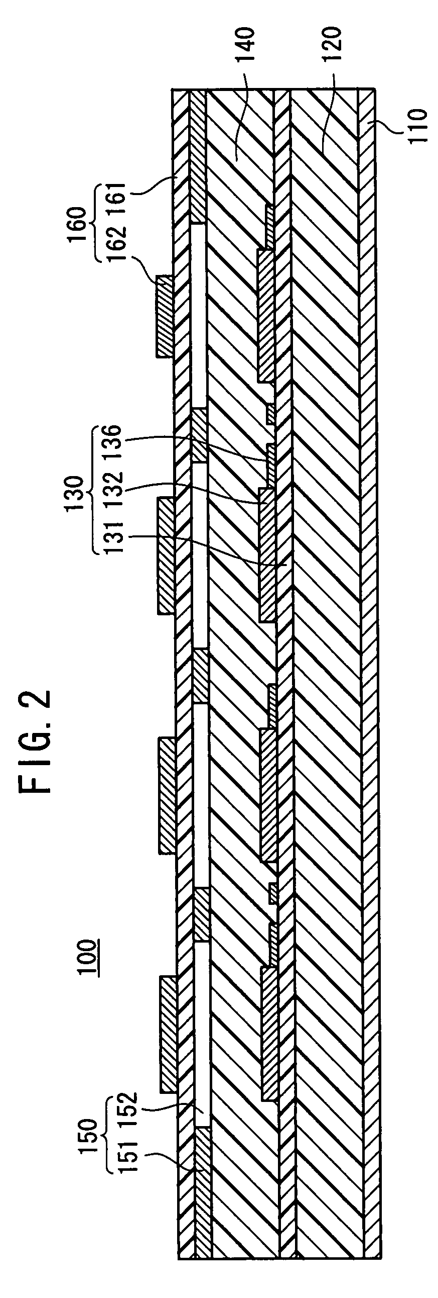
[0032]FIG. 1 is a plan view of a triplate planar slot antenna 100 according to an embodiment of the present invention. FIG. 2 is a sectional view taken along line II-II of FIG. 1, and FIG. 3 is an exploded perspective view of the triplate planar slot antenna 100.

[0033]As shown in FIGS. 2 and 3, the triplate planar slot antenna 100 is made up of a structure formed by successively laminating, starting from the bottom side thereof, a ground plate 110, a lower side dielectric layer 120, a lower side copper clad film substrate 130, an upper side dielectric layer 140, a slot plate 150, and an upper side copper clad film substrate 160. The antenna 100 preferably has a working frequency ranging from 15 GHz to 40 GHz, depending on the size of the antenna, practical considerations, etc., wherein the antenna 100 is suitable for use as a planar antenna for FWA (Fixed Wireless Access), for example.

[0034]The ground plate 110 comprises a rectangular metal plate, which is placed at the bottom of th...


PUM


Abstract

A triplate planar slot antenna formed by laying a ground plate, a lower layer side dielectric layer, a lower layer side copper-clad film substrate, an upper layer side dielectric layer, a slot plate and an upper layer side copper-clad film substrate sequentially from the bottom side, wherein a lower layer side copper foil piece is secured to the surface of a lower layer side insulating film by a joining technique not using adhesive, and an upper layer side copper foil piece is secured to the surface of an upper layer side insulating film by a joining technique not using adhesive. In a state where the copper foil pieces are removed, each insulating film has a dielectric constant in the range of 2.0-4.0, a tan δ in the range of 0.001-0.01, and a thickness of 25 μm or less.

Description

RELATED APPLICATIONS[0001]This is a U.S. National Phase Application under 35 USC 371 of International Application PCT / JP2005 / 019419, filed on 21 Oct. 2005.[0002]1.Technical Field[0003]The present invention relates to a triplate planar slot antenna formed by successively laminating, starting from the bottom side thereof, a ground plate, a lower side dielectric layer, a lower side copper clad film substrate, an upper side dielectric layer, a slot plate and an upper side copper clad film substrate.[0004]2.Background Art[0005]A conventional triplate planar slot antenna employs a structure formed by successively laminating, starting from the bottom side thereof, a ground plate, a lower side dielectric layer, a lower side copper clad film substrate, an upper side dielectric layer, a slot plate and an upper side copper clad film substrate.[0006]In the conventional triplate planar slot antenna, the lower side copper clad film substrate comprises a lower side insulating film and a plurality ...

Claims


Application Information

Patent Timeline
Patent Type & Authority Patents(United States)
IPC IPC(8): H01Q13/10H01Q1/38
CPCH01Q9/0414H01Q21/0006H01Q5/50H01Q21/065H01Q21/064
Inventor MIURA, YOHEIKAZAMA, YASUHIRO
Owner JAPAN RADIO CO LTD
Why Eureka
Try Eureka