Manufacturing a microlens at the extremity of a lead waveguide

a lead waveguide and microlens technology, applied in the field of optical microcomponents, can solve the problems of mechanical instability of adhesives, complex process of microlens alignment in front of optical fibers, and inability to meet the requirements of optical fibers

Inactive Publication Date: 2009-01-06
LUMENTUM D O O OPTICNA VLAKNA
View PDF9 Cites 19 Cited by
  • Summary
  • Abstract
  • Description
  • Claims
  • Application Information

AI Technical Summary

Benefits of technology

[0034]Advantageously, the present invention and its preferred embodiments provide unique and low-cost manufacturing processes allowing the assembly and the shaping of microlens of a variety of designs.

Problems solved by technology

It is known in the art that due to the size and to the shape of such devices, the process of microlens alignment in front of an optical fiber is very complex, always expensive and in many cases an impractical task.
Beside the constraints for selecting such adhesive in relation to their adhesion and optical properties, the main problem of this approach is the mechanical instability of the adhesives with time and temperature, which is unacceptable as microlenses are usually used in devices where positioning is critical.
The use of polymeric adhesives is therefore problematic since they have increased temperature dependence and are also susceptible to other environmental factors such as the presence of organic vapors that could make them swell or shrink or modify their optical properties, usually by reducing their light transmission, not mentioning the fact that they are often aging with time and are also frequently degraded by high light power (usually in the short energetic wavelength range) and by high temperature.
Some inorganic adhesives such as low melting point solder glasses could alternatively be used for demanding applications, but they have also their limitations and create problems associated with residual thermal stresses.
For applications where high light intensity and high temperature could be generated, such as in applications with fiber high power solid state lasers, the use of adhesives for microlens assembly could be in some cases problematic.
Although those polymeric microlenses may have interesting optical properties and advantages, such as for some techniques the possibility of custom surface shaping, their long term use and their temperature resistance is compromised due to the polymeric material used in their design.
Although a precise micromachining allows the shaping of interesting microlens profiles such as hyperbolic shapes, such techniques are complicated and not well suited for low-cost and high volume microlens manufacturing.
For all methods involving shaping or creating the glass microlens with heat, the size of the microlens could in some cases exceed the diameter of the optical fiber and the shape of the microlens is often difficult to control accurately.
The main drawbacks of these methods are limited repeatability and time-consuming fabrication process that requires individual machining of each produced microlens.
However there are only few examples in the literature applying this concept for shaping glass microlenses at the tip of an optical fiber.
They also showed a slight increase of coupling efficiency between a fiber with a microlens and a laser diode, but the technique remained undeveloped and it does not allow for the realization of a microlens with arbitrary size and appropriate quality.

Method used


Image

  • Manufacturing a microlens at the extremity of a lead waveguide
  • Manufacturing a microlens at the extremity of a lead waveguide
  • Manufacturing a microlens at the extremity of a lead waveguide

Examples


Embodiment Construction

[0051]In the following description, similar features in the drawings have been given similar reference numerals and in order to weight down the figures, some elements are not referred to in some figures if they were already identified in a precedent.

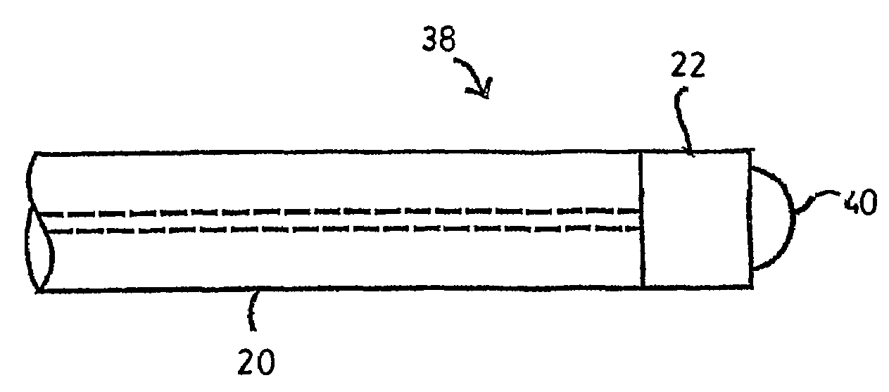
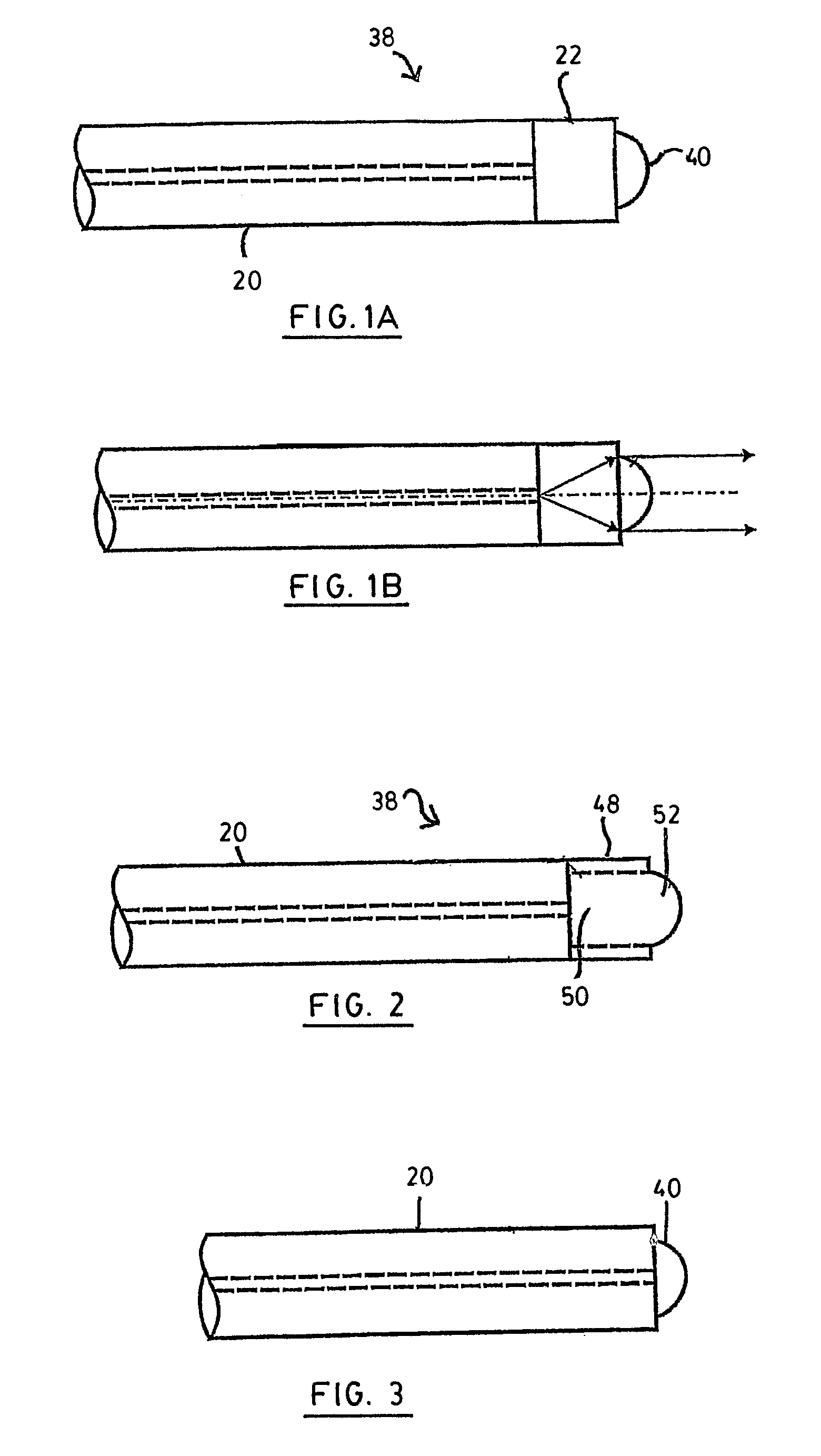
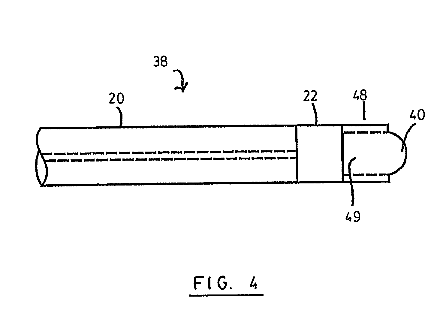
[0052]The present invention first provides various methods for the fabrication of a microlens at an extremity of a lead waveguide. As will be apparent from the description below, the present method may be used to produce a resulting microlens of any one of a variety of desired shapes.

[0053]For convenience, throughout the present specification, the various embodiments of methods and assemblies according to the invention will be described using an optical fiber as the lead waveguide. It is however understood that the present invention may be easily adapted to planar or other types of wave guiding structures from which light may need to be coupled, and that such devices are clearly considered within the scope of the present invention.

[0054]...


PUM

PropertyMeasurementUnit
spacer lengthaaaaaaaaaa
sizeaaaaaaaaaa

Abstract

Variants of a method for manufacturing a microlens of any desired shape at the extremity of a lead waveguide are provided. A lens element having a non-uniform radial etchability profile is provided at the extremity of the lead waveguide. Preferably, the etchability profile is determined by a non-uniform radial distribution of dopants in the lens element. A spacer may optionally be placed between the waveguide and the lens element. The lens element is then brought down to an appropriate length and etched to its final shape which is mainly determined by the dopant distribution. An optical coupling assembly having a non-uniform radial distribution of dopants therein is also provided.

Description

RELATED APPLICATIONS[0001]This application is the U.S. National Phase under 35 U.S.C. 371 of International Application No. PCT / CA2005 / 001290, filed on Aug. 25, 2005, which in turn claims the benefit of Slovenian Patent Application No. P 200400234SI, filed on Aug. 25, 2004, the disclosures of which Applications are incorporated by reference herein.FIELD OF THE INVENTION[0002]The present invention relates to the field of optical micro-components and more preferably concerns the provision of a microlens at the extremity of a lead waveguide.BACKGROUND OF THE INVENTION[0003]With the development of micro-optics and all-fiber technologies mainly driven by the telecommunication industry, there is an increased need for miniaturized optics and especially miniaturized optical devices that could be simply assembled with optical waveguides in general and optical fibers in particular. Among those devices, microlenses are of particular interest. The field of microlenses combined with optical fibe...

Claims


Application Information

Patent Timeline
Patent Type & Authority Patents(United States)
IPC IPC(8): G02B6/32B29D11/00G02B6/26
CPCG02B6/262B29D11/00692
Inventor DONLAGIC, DENISCIBULA, EDVARDPINET, ERIC
Owner LUMENTUM D O O OPTICNA VLAKNA
Why Eureka
Try Eureka