

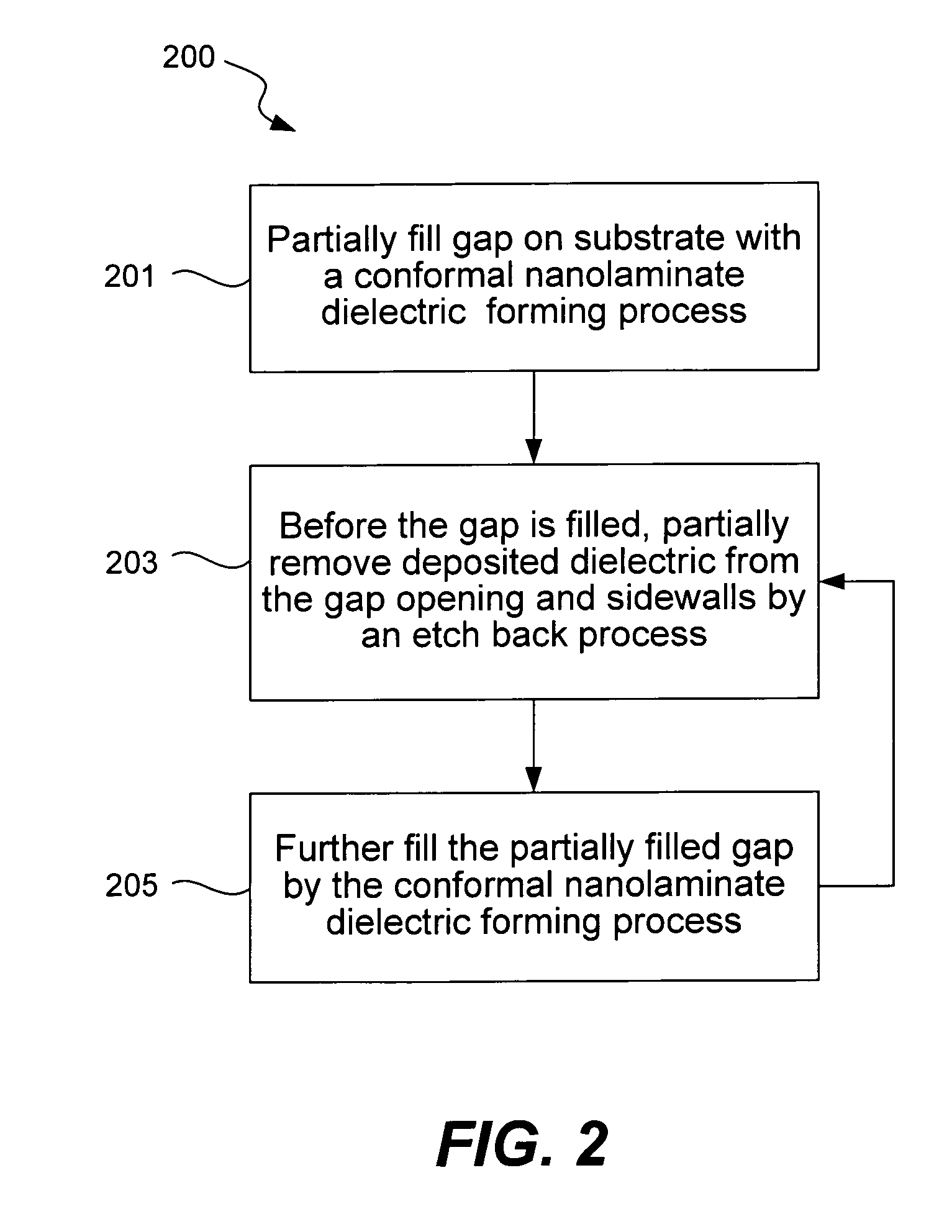
Conformal nanolaminate dielectric deposition and etch back gap fill process
a dielectric layer and nanolaminate technology, applied in chemical vapor deposition coatings, coatings, metallic material coating processes, etc., can solve the problems of void-free filling of high aspect ratio spaces (e.g., ar>3.0:1) becoming increasingly difficult, and the dimension shrinking, etc., to achieve the effect of reducing the incidence of voids or weak spots
- Summary
- Abstract
- Description
- Claims
- Application Information
AI Technical Summary
Benefits of technology
Problems solved by technology
Method used
Image

Examples
Embodiment Construction
[0019]Reference will now be made in detail to specific embodiments of the invention. Examples of the specific embodiments are illustrated in the accompanying drawings. While the invention will be described in conjunction with these specific embodiments, it will be understood that it is not intended to limit the invention to such specific embodiments. On the contrary, it is intended to cover alternatives, modifications, and equivalents as may be included within the spirit and scope of the invention as defined by the appended claims. In the following description, numerous specific details are set forth in order to provide a thorough understanding of the present invention. The present invention may be practiced without some or all of these specific details. In other instances, well known process operations have not been described in detail in order not to unnecessarily obscure the present invention.
Introduction
[0020]The present invention relates to conformal nanolaminate dielectric (e....
PUM
| Property | Measurement | Unit |
|---|---|---|
| aspect ratio | aaaaa | aaaaa |
| aspect ratio | aaaaa | aaaaa |
| temperatures | aaaaa | aaaaa |
Abstract
Description
Claims
Application Information