Surface-emitting type semiconductor laser and method for manufacturing the same

a surface-emitting type, semiconductor laser technology, applied in semiconductor lasers, laser details, electrical equipment, etc., can solve the problems of difficult control of polarization planes of surface-emitting type semiconductor lasers, and inability to uniformly distribute current density, so as to achieve high reliability and achieve the effect of not lowering energy usage efficiency

Inactive Publication Date: 2009-02-03
SEIKO EPSON CORP
View PDF34 Cites 0 Cited by
  • Summary
  • Abstract
  • Description
  • Claims
  • Application Information

AI Technical Summary

Benefits of technology

[0009]Exemplary aspects of the present invention provide a highly reliable surface-emitting type semiconductor laser and a method for manufacturing the same, which is capable of controlling polarization planes without lowering the energy usage efficiency.
[0011]According to the surface-emitting type semiconductor laser, a planar configuration of the second columnar section has anisotropy. Accordingly, anisotropy to confine light can be obtained in the second columnar section. The anisotropy of the planar configuration of the second columnar section makes it possible to control the polarization direction of laser that is emitted.
[0012]Also, according to the surface-emitting type semiconductor laser, an electric current flows generally uniformly in the columnar section, particularly in a region adjacent to the active layer. Since almost no offset occurs in the current density distribution in the first columnar section, the energy usage efficiency is high.
[0013]Accordingly, by the surface-emitting type semiconductor laser, the polarization direction of laser light can be controlled while maintaining the energy usage efficiency.

Problems solved by technology

However, the control of polarization planes of a surface-emitting type semiconductor laser is difficult because of the symmetry of its planar structure.
Therefore, when a surface-emitting type semiconductor laser is used for an optical system with a polarization dependence, instability of polarization planes causes noise.
However, according to these methods, the current density distribution is not uniform, and the energy usage efficiency may be lowered.
However, according to this method, SiN is formed on the side surface of the resonator 140 at different temperatures in order to add anisotripic strain to the active layer, which complicates the process.
Furthermore, according to this method, the planar configuration of the resonator 140 is practically limited to a quadrilateral shape to obtain sufficient effectiveness in controlling polarization planes.
A circular planar configuration does not demonstrate effectiveness in controlling polarization planes.
In this case, the oxide layer structure adjacent to the active layer and oxidation process are complicated, and the service life of the device may be adversely affected.

Method used


Image

  • Surface-emitting type semiconductor laser and method for manufacturing the same
  • Surface-emitting type semiconductor laser and method for manufacturing the same
  • Surface-emitting type semiconductor laser and method for manufacturing the same

Examples


first exemplary embodiment

1. First Exemplary Embodiment

1-1 Device Structure

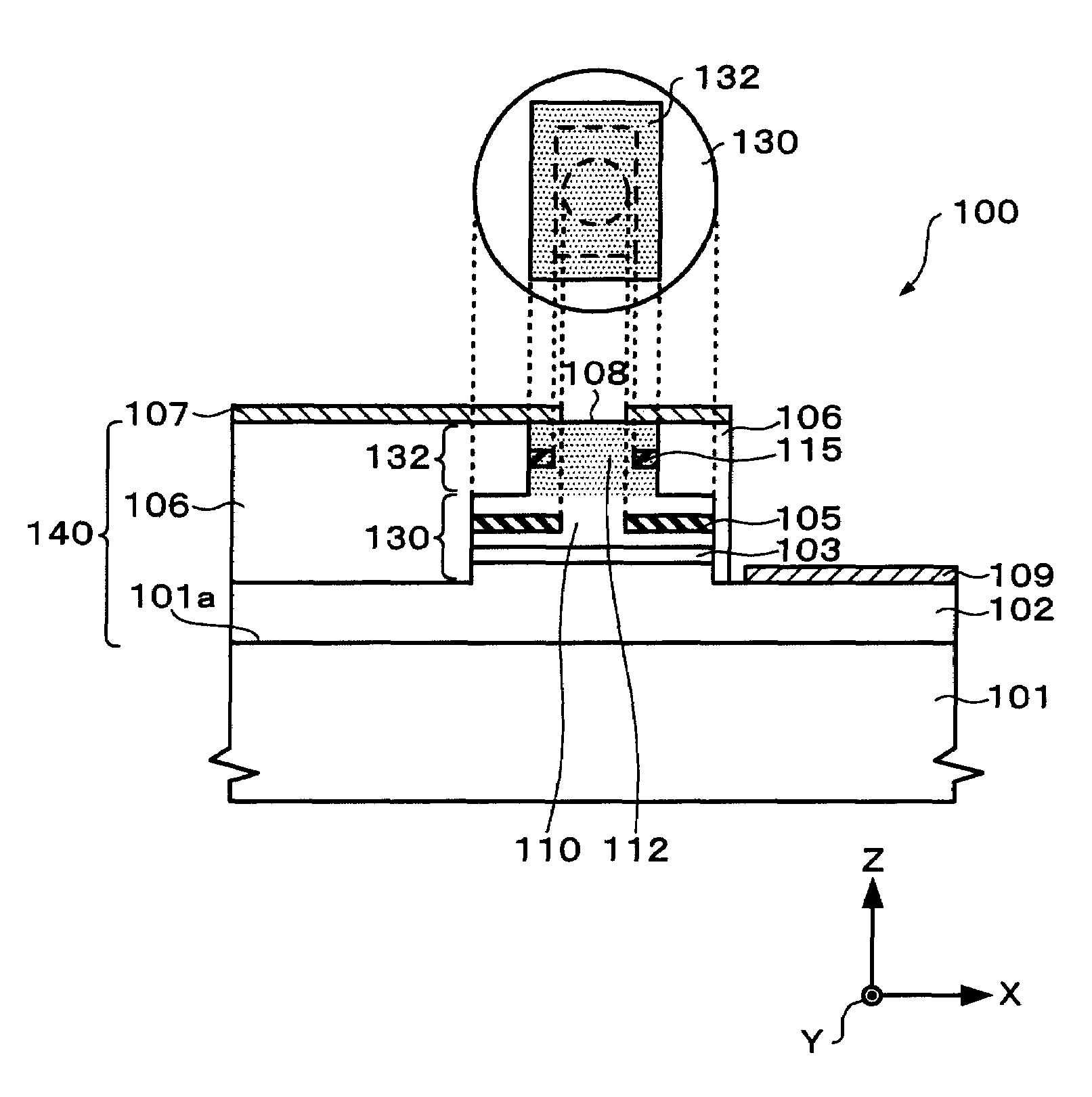
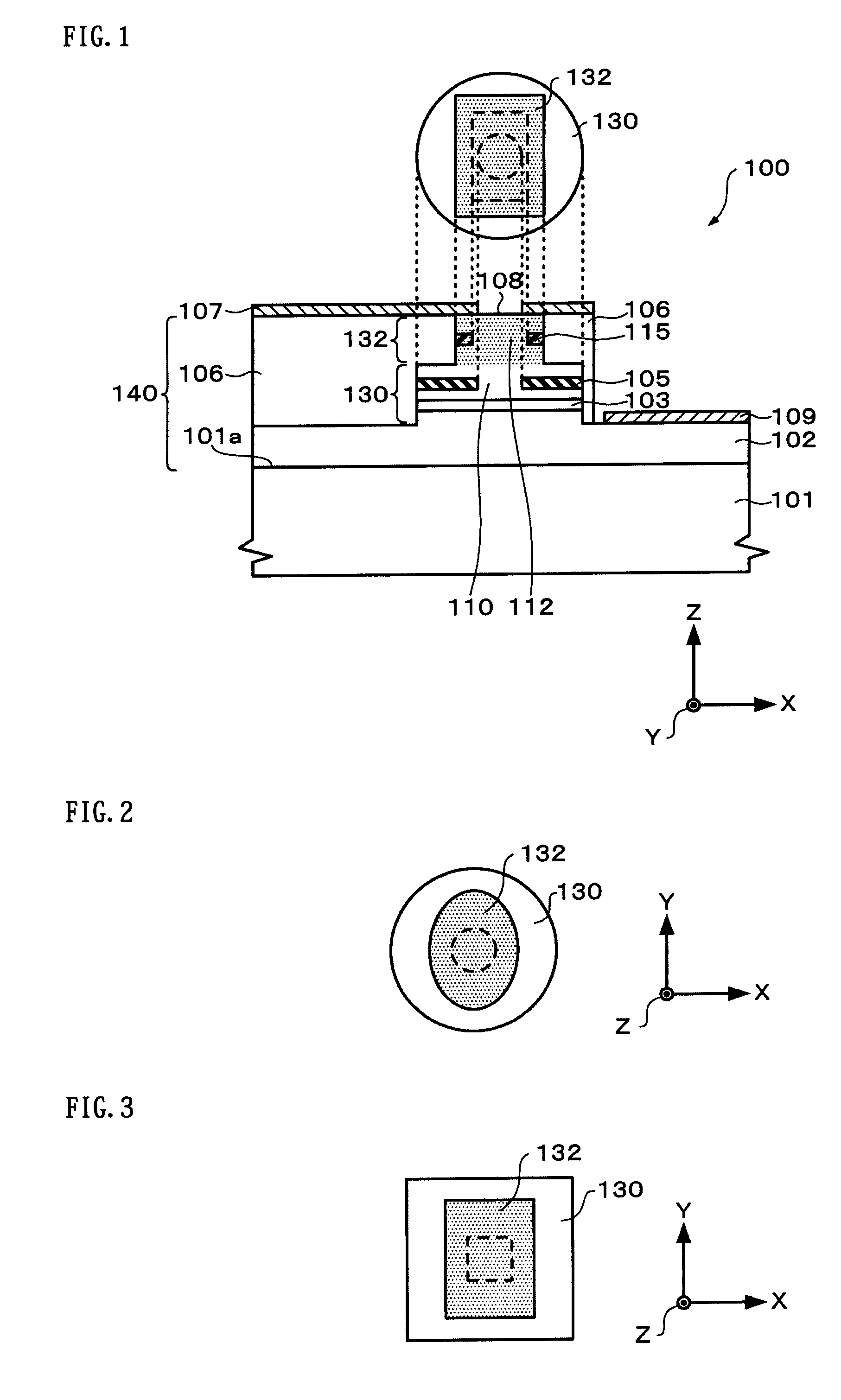
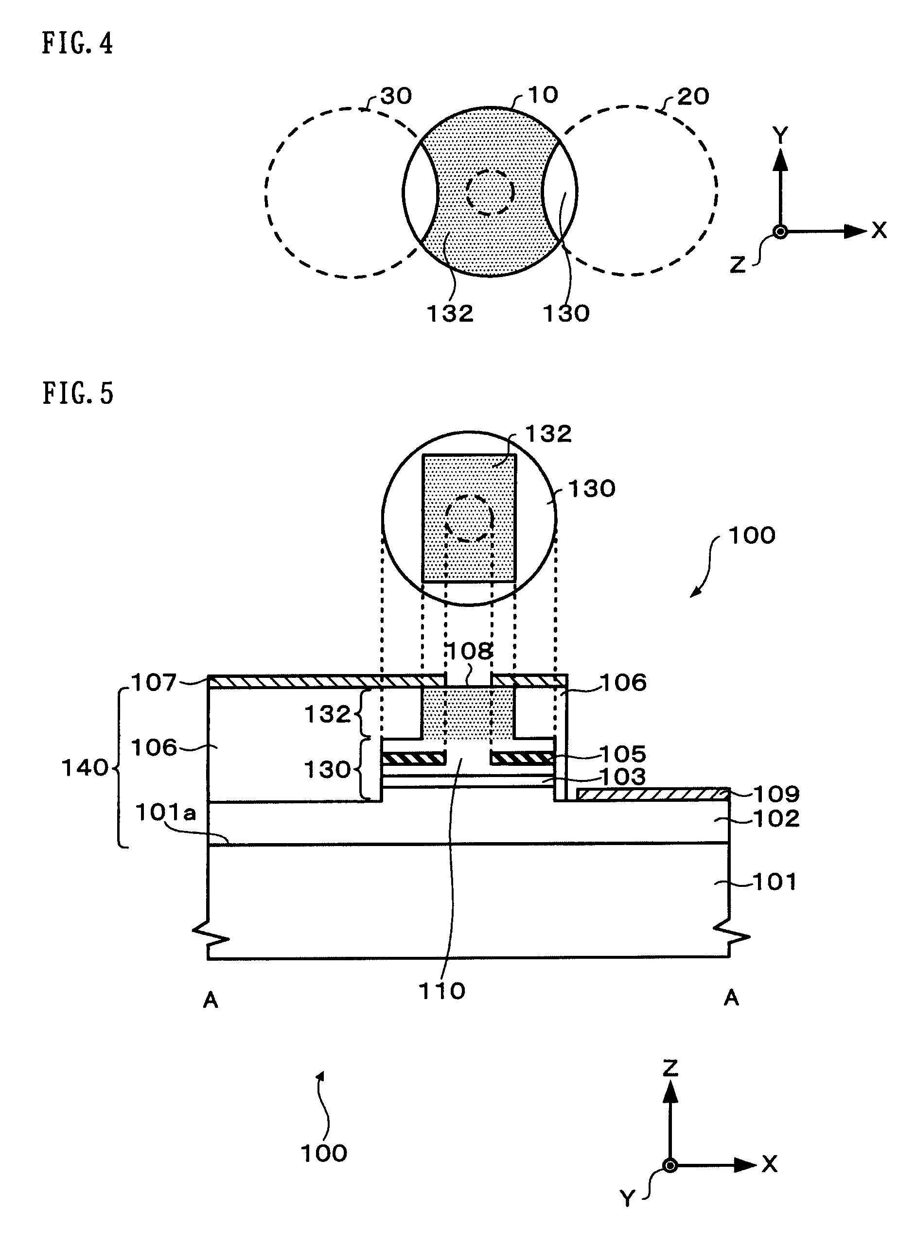
[0054]FIG. 1 is a schematic of a surface-emitting type semiconductor laser (hereinafter “surface emitting laser”) 100 in accordance with a first exemplary embodiment of the present invention. FIG. 2-FIG. 4 are schematics of major portions of the surface-emitting laser 100 of the first exemplary embodiment.

[0055]The surface emitting laser 100 according to the first exemplary embodiment of the present invention includes a semiconductor substrate (a GaAs substrate in accordance with the present exemplary embodiment) 101, a vertical-cavity resonator 140 (hereinafter “resonator 140”) formed on the semiconductor substrate 101, a first electrode 107 and a second electrode 109. The resonator 140 includes a first mirror 102, an active layer 103, and a second mirror 104.

[0056]Next, each of the compositions of the surface-emitting laser 100 will be described.

[0057]The resonator 140 may be formed, for example, from a first mirror 102 that is a di...

second exemplary embodiment

2. Second Exemplary Embodiment

2-1 Device Structure

[0105]FIG. 14 is a schematic of a surface emitting laser 200 in accordance with a second exemplary embodiment of the present invention. FIG. 15-FIG. 17 are schematics of major portions of the surface-emitting laser 200 in accordance with the second exemplary embodiment. The same reference numerals are appended to components that have substantially the same functions as those of the surface-emitting laser 100 in accordance with the first exemplary embodiment, and their detailed description is omitted.

[0106]As shown in FIG. 14, the surface-emitting laser 200 of the present exemplary embodiment includes a semiconductor substrate (a GaAs substrate in the present embodiment) 101, a resonator 140 formed on the semiconductor substrate 101, a first electrode 107, and a second electrode 109. The resonator 140 includes a first mirror 102, an active layer 103, and a second mirror 104.

[0107]The second mirror 104 includes a part of a first column...


PUM


Abstract

A surface-emitting type semiconductor laser includes a substrate; a first mirror disposed above the substrate; an active layer disposed above the first mirror; a second mirror disposed above the active layer; a first columnar section including the active layer, the first columnar section not having anisotropy; a first dielectric layer disposed in the first columnar section, the first dielectric layer including a symmetric opening section; a second columnar section disposed above the first columnar section, the second columnar section having an outer wall that has anisotropy; and a second dielectric layer disposed in the second columnar section, the second dielectric layer including an asymmetric opening section.

Description

[0001]The present application claims priority to Japanese Patent Application No. 2003-320038 filed Sep. 11, 2003, which is hereby expressly incorporated by reference herein in its entirety.BACKGROUND OF THE INVENTION[0002]1. Field of Invention[0003]Exemplary aspects of the present invention relate to a surface-emitting type semiconductor laser and a method for manufacturing the same.[0004]2. Description of Related Art[0005]A surface emitting semiconductor laser is a semiconductor laser which emits laser light in a direction perpendicular to a semiconductor substrate. Surface emitting type semiconductor lasers have excellent characteristics including, for example, easy handling, low threshold currents, etc., compared to related art edge emitting semiconductor lasers. Thus, this technology may be applied to a variety of sensors and light sources for optical communications. However, the control of polarization planes of a surface-emitting type semiconductor laser is difficult because o...

Claims


Application Information

Patent Timeline
Patent Type & Authority Patents(United States)
IPC IPC(8): H01S5/00H01S5/183H01S5/042H01S5/343
CPCB82Y20/00H01S5/18338H01S5/0425H01S5/18313H01S5/18316H01S5/18333H01S5/18341H01S5/18347H01S5/18355H01S5/3432H01S2301/18H01S5/04257H01S5/18394
Inventor KANEKO, TSUYOSHIIDE, TSUGIONAKAYAMA, HITOSHI
Owner SEIKO EPSON CORP
Why Eureka
Try Eureka