Liquid crystal display device and fabricating method thereof

a technology of liquid crystal display and fabrication method, which is applied in the direction of semiconductor devices, instruments, optics, etc., can solve the problems of complex fabrication process and major component of the manufacturing cost of the liquid crystal display panel

Inactive Publication Date: 2009-02-10
LG DISPLAY CO LTD
View PDF11 Cites 13 Cited by
  • Summary
  • Abstract
  • Description
  • Claims
  • Application Information

AI Technical Summary

Benefits of technology

[0014]An advantage of the present invention is to provide a thin film transistor substrate that is adaptive for simplifying process, and a fabricating method thereof.

Problems solved by technology

The thin film transistor substrate includes a semiconductor process and requires a plurality of mask processes, thus its fabricating process is complicated and it becomes a major component of the manufacturing cost of the liquid crystal display panel.

Method used


Image

  • Liquid crystal display device and fabricating method thereof
  • Liquid crystal display device and fabricating method thereof
  • Liquid crystal display device and fabricating method thereof

Examples


Embodiment Construction

[0030]Reference will now be made in detail to the preferred embodiments of the present invention, examples of which are illustrated in the accompanying drawings.

[0031]With reference to FIGS. 2 to 9F, embodiments of the present invention will be explained as follows.

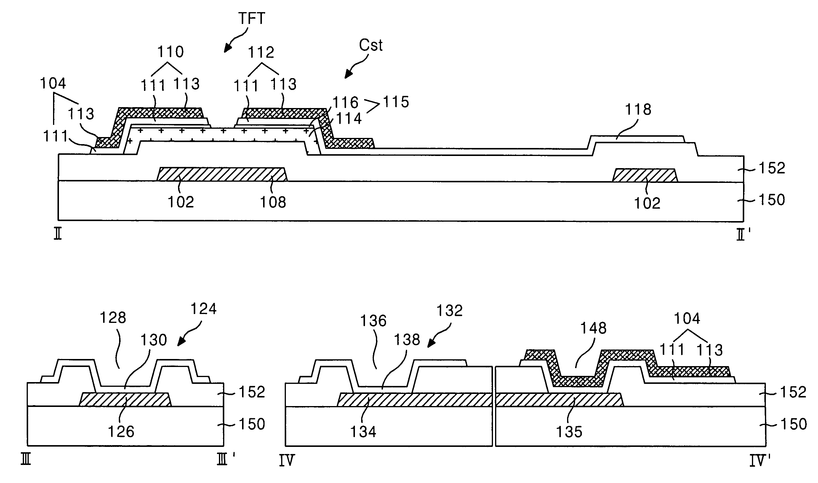
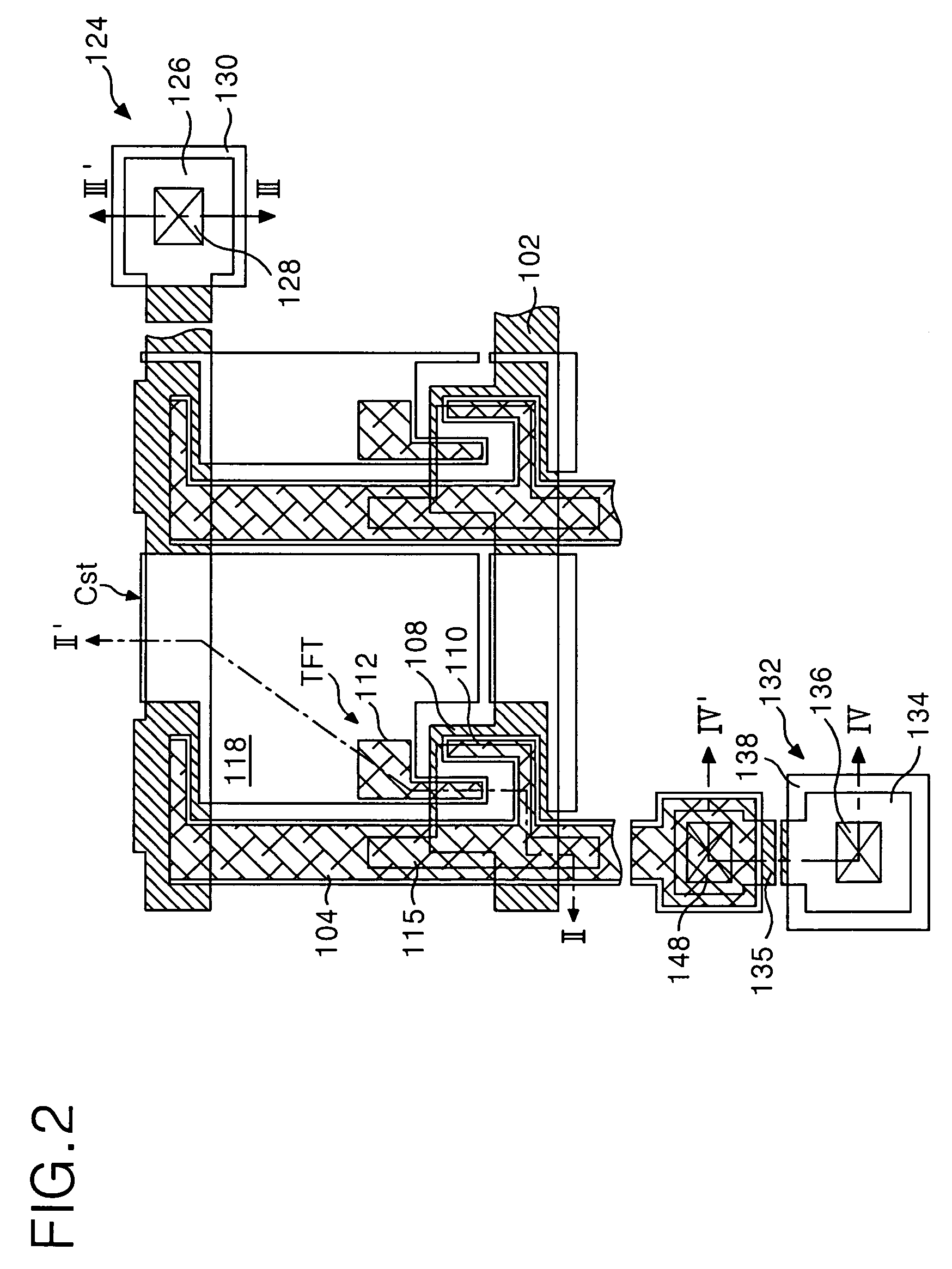
[0032]FIG. 2 is a plan view illustrating a thin film transistor substrate according to an embodiment of the present invention, and FIG. 3 is a cross-sectional view illustrating the thin film transistor substrate shown in FIG. 2, taken along the lines III-III′, IV-IV′, V-V′, VI-VI′.

[0033]The thin film transistor substrate shown in FIGS. 2 and 3 includes: a gate line 102 and a data line 104 that are formed on a lower substrate 150 crossing each other with a gate insulating film 152 therebetween to define a pixel area; a thin film transistor TFT connected to the gate line 102, the data line 104, and a pixel electrode 118; and the pixel electrode 118 connected to the thin film transistor TFT; and a storage capacitor Cst forme...


PUM

PropertyMeasurementUnit
areaaaaaaaaaaa
transparentaaaaaaaaaa
conductiveaaaaaaaaaa

Abstract

A liquid crystal display device, including: a gate line on a substrate; a data line crossing the gate line with a gate insulating film in between to define a pixel area; a thin film transistor having a gate electrode connected to the gate line, a source electrode connected to the data line, a drain electrode facing the source electrode, and a semiconductor pattern providing a channel between the source electrode and the drain electrode; and a pixel electrode in the pixel area connected to the drain electrode, wherein the data line, the source electrode, and the drain electrode are formed of a first conductive layer group of double conductive layers, the pixel electrode is formed of the lowermost layer of the extended drain electrode, and the data line, the source electrode, the drain electrode, and the pixel electrode are in an area that is to be sealed by a sealant.

Description

[0001]This application claims the benefit of the Korean Patent Application No. P2004-112587 filed on Dec. 24, 2004, which is hereby incorporated by reference for all purposes as if fully set forth herein.BACKGROUND OF THE INVENTION[0002]1. Field of the Invention[0003]The present invention relates to a liquid crystal display device, and more particularly to a thin film transistor substrate that simplifies a fabricating method thereof.[0004]2. Discussion of the Related Art[0005]A liquid crystal display device controls the light transmittance of liquid crystal having dielectric anisotropy by use of an electric field, thereby displaying a picture. The liquid crystal display device includes a liquid crystal display panel for displaying picture through a liquid crystal cell matrix and a drive circuit to drive the liquid crystal display panel.[0006]Referring to FIG. 1, a liquid crystal display panel of the related art includes a color filter substrate 10 and a thin film transistor substrat...

Claims


Application Information

Patent Timeline
Patent Type & Authority Patents(United States)
IPC IPC(8): G02F1/1343
CPCG02F1/136286H01L29/66765H01L27/124H01L27/1288G02F1/1339G02F2001/136231G02F2001/13629G02F2201/123H01L27/12G02F1/136231G02F1/13629G02F1/136
Inventor AHN, BYUNG CHULPARK, BYUNG HOPARK, JONG HYUN
Owner LG DISPLAY CO LTD
Why Eureka
Try Eureka