Eureka AIR delivers breakthrough ideas for toughest innovation challenges, trusted by R&D personnel around the world.

Reduction of leakage current and program disturbs in flash memory devices

a flash memory device and leakage current technology, applied in the field can solve the problems of parasitic leakage current increasing the required programming current by tens of microamperes, affecting the operation of flash memory devices, so as to reduce the amount of electron diffusion

Inactive Publication Date: 2009-02-10
MONTEREY RES LLC
View PDF15 Cites 9 Cited by
  • Summary
  • Abstract
  • Description
  • Claims
  • Application Information

AI Technical Summary

Benefits of technology

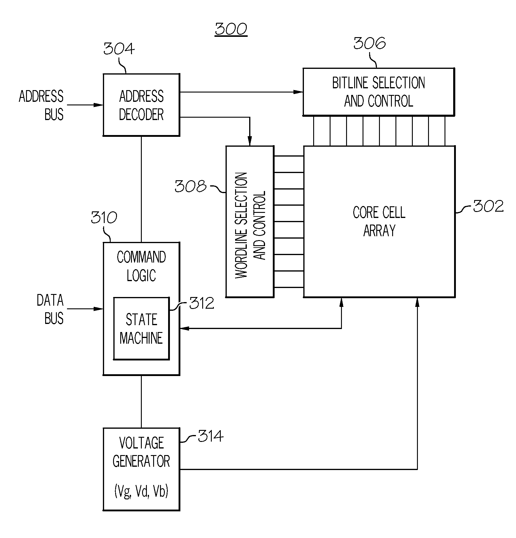
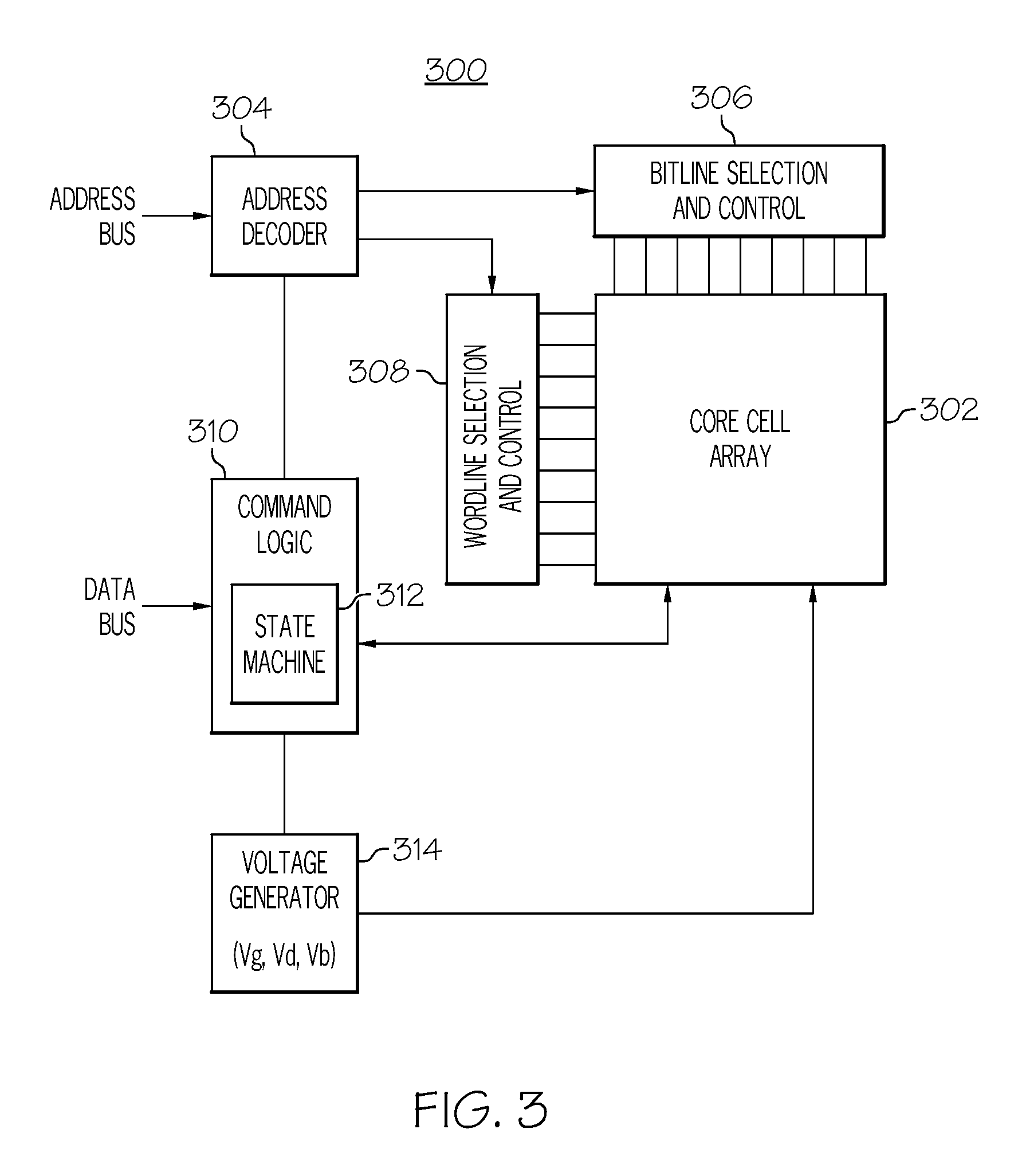
[0012]A flash memory programming technique as described herein can be utilized with memory cells arranged in a virtual ground architecture. The programming technique reduces bitline leakage current during programming, which conserves power. The programming technique also reduces the number of program disturbs in the array. Various flash memory verification techniques as described herein can also be utilized with memory cells arranged in a virtual ground architecture. The verification techniques reduce the bitline leakage current component in the measured current, resulting in more accurate assessment of the actual verification current generated by the target cell.
[0015]The above and other aspects of the invention may also be carried out in one embodiment by a method of programming a nonvolatile memory device having an array of cells arranged in a virtual ground architecture, each cell including a gate corresponding to a wordline in the array, a selectable source / drain formed in a semiconductor substrate and corresponding to a bitline in the array, and a selectable drain / source formed in the semiconductor substrate and corresponding to a bitline in the array. The method involves: selecting a target cell in the array for programming; applying a programming voltage to the wordline corresponding to the target cell; applying a drain bias voltage to a first selectable bitline corresponding to the drain of the target cell; and applying a negative substrate bias voltage to the semiconductor substrate of the target cell to reduce electron diffusion below the first selectable bitline during programming.

Problems solved by technology

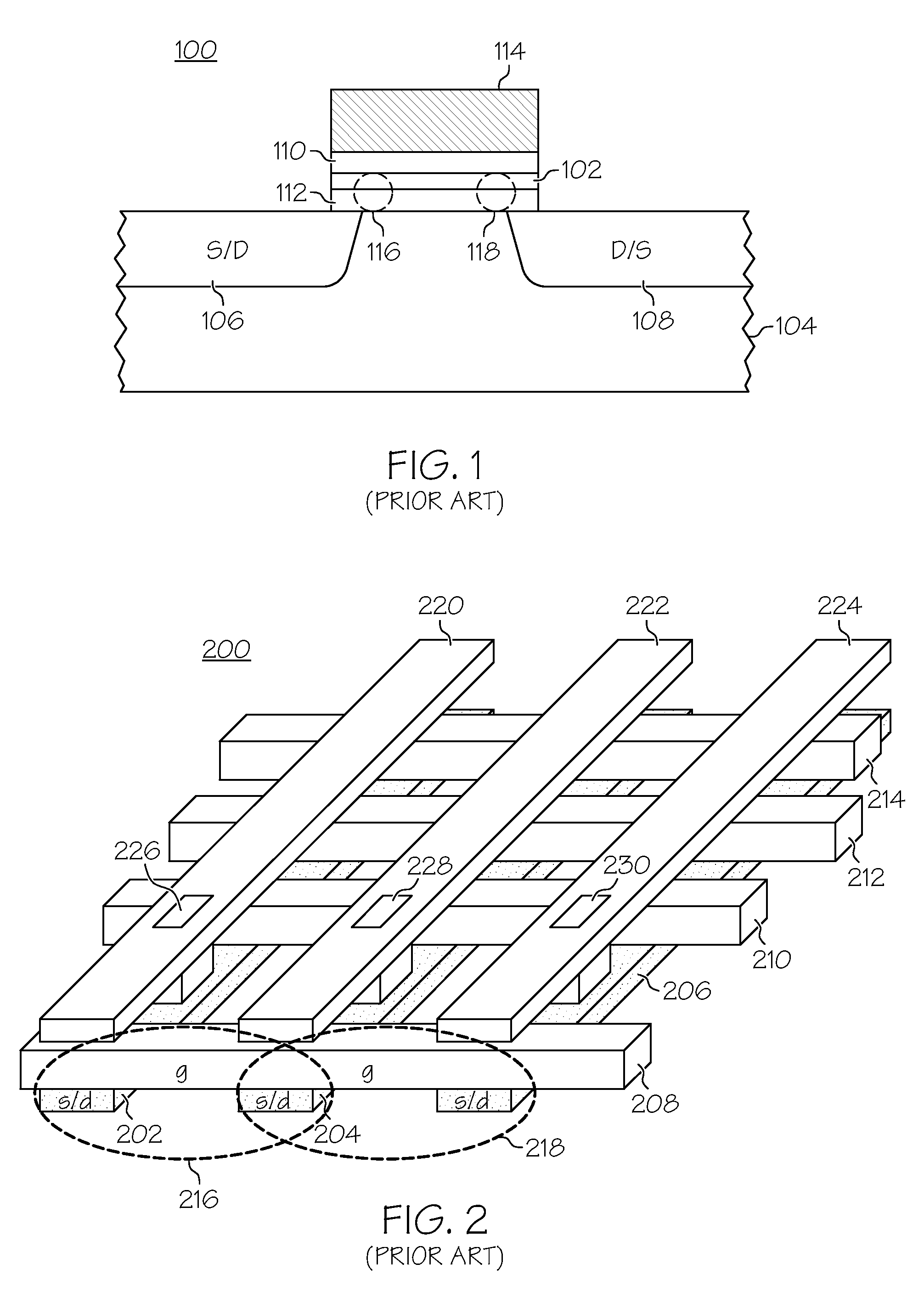
Referring again to FIG. 2, conventional CHE programming of a flash memory array arranged in a virtual ground architecture may result in excessive current leakage flowing under the unselected wordlines, between the wordlines, and in the bitline contact areas.
Such bitline leakage current can increase the required programming current by tens of microamperes, which is a significant amount considering the nominal operating characteristics of such a flash memory array.
Moreover, due to natural degradation of the cells, the amount of this parasitic leakage current can increase by roughly two orders of magnitude (100×) after the array has experienced many program-erase cycles.
Excessive leakage current can be very undesirable in low power applications such as portable electronic devices, wireless telephones, or the like.
Excessive leakage current may have other negative implications in a practical flash memory device, such as: reducing programming efficiency due to the IR drop along the bitlines from the excess current, and disturb of cells on unselected wordlines due to the presence of channel current on the unselected wordlines.
Bitline leakage current, even in small amounts, can introduce errors in the verification operation because the measurement circuitry measures the actual verification current combined with any leakage current.
Moreover, as flash memory devices are scaled down and the channel length of the memory cells is reduced, program disturbs of adjacent devices also increase.
Another kind of program disturb may occur in adjacent memory cells that share the same wordline as the memory cell being programmed.

Method used


Image

  • Reduction of leakage current and program disturbs in flash memory devices
  • Reduction of leakage current and program disturbs in flash memory devices
  • Reduction of leakage current and program disturbs in flash memory devices

Examples


Embodiment Construction

[0025]The following detailed description is merely illustrative in nature and is not intended to limit the embodiments of the invention or the application and uses of such embodiments. Furthermore, there is no intention to be bound by any expressed or implied theory presented in the preceding technical field, background, brief summary or the following detailed description.

[0026]Embodiments of the invention may be described herein in terms of functional and / or logical block components and various processing steps. It should be appreciated that such block components may be realized by any number of hardware, software, and / or firmware components configured to perform the specified functions. For example, an embodiment of the invention may employ various integrated circuit components, e.g., memory elements, digital signal processing elements, logic elements, look-up tables, or the like, which may carry out a variety of functions under the control of one or more microprocessors or other ...


PUM


Abstract

A flash memory system configured in accordance with an example embodiment of the invention employs a virtual ground array architecture. During programming operations, target memory cells are biased with a negative substrate bias voltage to reduce or eliminate leakage current that might otherwise conduct through the target memory cells. The negative substrate bias voltage also reduces the occurrence of program disturbs in cells adjacent to target cells by extending the depletion region deeper below the bit line that corresponds to the drain of the target device. The negative substrate bias voltage may also be applied to target memory cells during verification operations (program verify, soft program verify, erase verify) to reduce or eliminate leakage current that might otherwise introduce error in the verification operations.

Description

TECHNICAL FIELD[0001]Embodiments of the present invention relate generally to flash memory devices. More particularly, embodiments of the present invention relate to the programming and verification operations for flash memory devices.BACKGROUND[0002]Flash memory is a type of electronic memory media that can hold its data in the absence of operating power. Flash memory can be programmed, erased, and reprogrammed during its useful life (which may be up to one million write cycles for typical flash memory devices). Flash memory is becoming increasingly popular as a reliable, compact, and inexpensive nonvolatile memory in a number of consumer, commercial, and other applications. As electronic devices get smaller and smaller, it becomes desirable to increase the amount of data that can be stored per unit area on an integrated circuit memory element, such as a flash memory unit. In this regard, one conventional flash memory technology is based upon a memory cell that utilizes a charge tr...

Claims


Application Information

Patent Timeline
Patent Type & Authority Patents(United States)
IPC IPC(8): G11C11/34
CPCG11C5/146G11C16/0475G11C16/10G11C16/3427G11C16/3436G11C16/3445G11C16/3459G11C29/02G11C29/021G11C29/028G11C16/04G11C16/0491G11C16/08G11C16/12G11C16/3409G11C16/3418
Inventor CHANG, KUO-TUNGTHURGATE, TIMOTHY
Owner MONTEREY RES LLC
Why Eureka
Eureka Blog
Learn More