Method and apparatus for image processing

a technology of image data and processing method, applied in the field of image data processing, can solve the problems of conventional computational systems becoming less effective for large-scale real-time image processing, systems with a limited throughput, and conventional computational systems deficien

Inactive Publication Date: 2009-02-10
PARIMICS
View PDF8 Cites 16 Cited by
  • Summary
  • Abstract
  • Description
  • Claims
  • Application Information

AI Technical Summary

Benefits of technology

[0012]Prior to being processed, images are captured via an image capturing device that may be a charged coupled device (CCD) and formed on a first semiconductor substrate. One ore more analog-to-digital converters may also be formed on the first semiconductor substrate to convert the captured analog image data to digital data. A realignment buffer realigns the data received from the analog-to-digital converters. The plurality of processors corresponding to the first layer are formed on a second semiconductor substrate that is separate from the first semiconductor substrate.

Problems solved by technology

Conventional computational systems are becoming increasingly less effective for large scale real time image processing.
Conventional computational systems are also deficient when image processing is carried out for two or more spatial dimensions.
This results in systems with a limited throughput.
Such conventional image processing systems are often unable to provide the required processing speed if, for example, the frame rate is high, or the required resolution is high, or the total pixel count and the color depth per pixel is high, or the number of CPU instructions per pixel is high.
This processing limitation is caused, in part, by the fact that the CPUs cannot access image data fast enough from the memory (i.e., DRAM) and / or fetch code from the DRAM subsystem.
Multiprocessor systems have been developed and deployed but because accesses to the DRAMs are limited due to contention and blocking, these systems are unable to process the frames at the required rates.
This problem is further compounded by the fact that the image processing requirement for a two-dimensional image with N×M pixels (typically M=3×N / 4 or M=4×N / 5) is a linear function of N2.
The architecture of image processing system 10 is relatively inexpensive and can be built with standard parts and off-the-shelf processors; however, it has a limited throughput.
Despite their ever-increasing CPU performance, conventional image processing systems are not fully effective at handling such high frame processing rates, partly due to the latency associated with the DRAMs.
However, this technique decreases the image quality since a significant portion of the chip area is not light sensitive and cannot capture images.
Also, because these CCD chips are formed on a DRAM-type process, the speed of the processing engine of such chips is often limited, particularly, if the processing engines were configured to be software programmable.
Moreover, the optical resolution of these chips deteriorates as the size of the co-located processing engines increases.
Furthermore, these chips are only capable of capturing images in the range of the visible light, and thus fail to capture and process images generated by SONAR, RADAR, or light detection and ranging (LIDAR), and all other frequency ranges of the electromagnetic spectrum of waves.
Because, as seen from FIG. 2, the granularity of the layers is limited, prior art image processing systems are unable to map specific image processing tasks to hardware dedicated to perform these tasks.

Method used


Image

  • Method and apparatus for image processing
  • Method and apparatus for image processing
  • Method and apparatus for image processing

Examples


Embodiment Construction

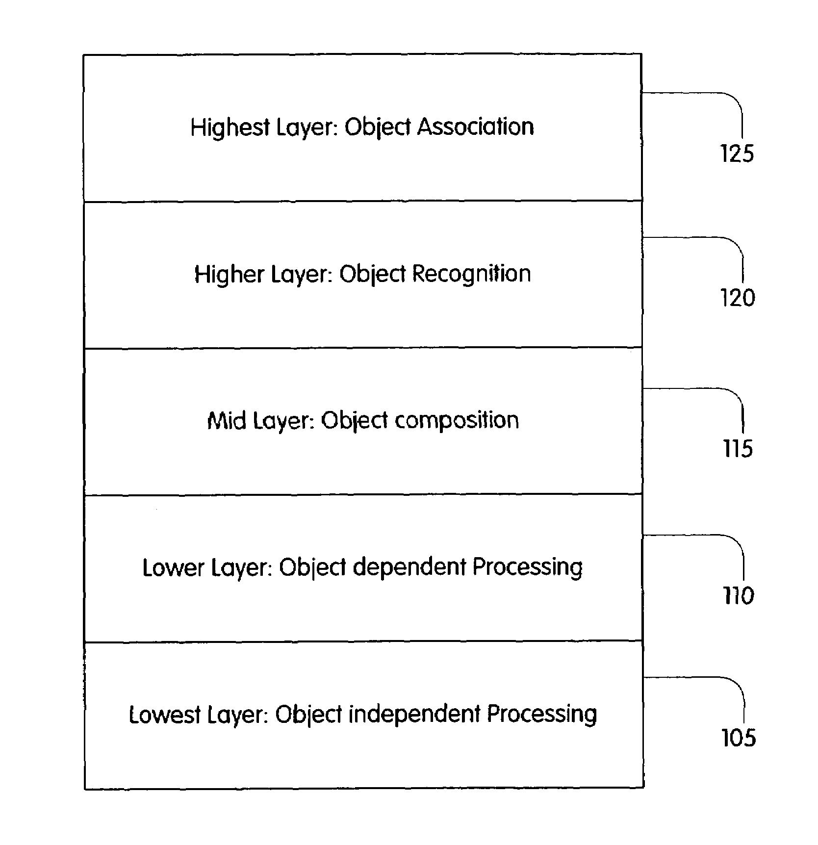
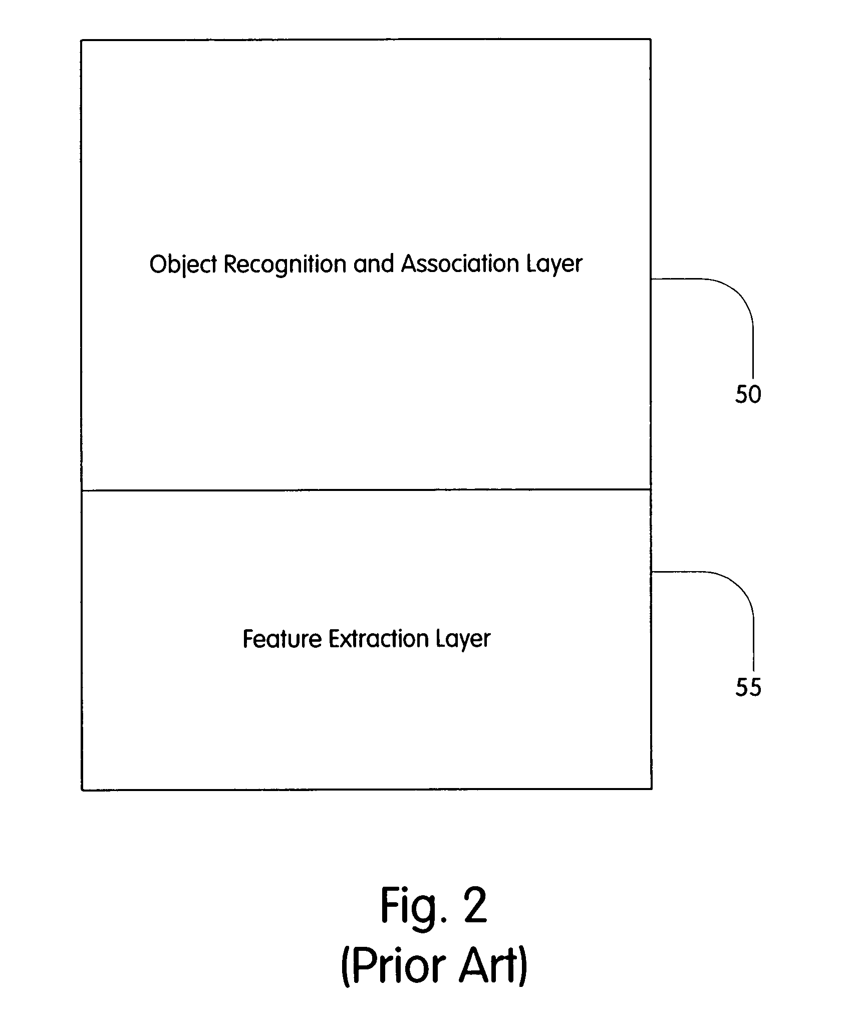
[0019]FIG. 3 shows various processing layers (alternatively referred to hereinbelow as layers) of an image processing system adapted to process images, in accordance with one embodiment of the present invention. The image processing system of the present invention is shown in FIG. 3 as including 5 layers, namely an object independent processing layer 105, an object dependent processing layer 110, an object composition layer 115, an object recognition layer 120, and an object association layer 125. It is understood that object composition layer 115, object recognition layer 120, and object association layer 125, in combination, correspond to object recognition and association layer 50, as shown in FIG. 2 and hence are not described below. It is further understood that object composition layer 115, object recognition layer 120, and object association layer 125 may be combined into, for example, two layers.

[0020]In accordance with the present invention, object independent processing la...


PUM


Abstract

An image processing system processes images via a first processing layer adapted to perform object-independent processing, a second processing layer adapted to perform object-dependent processing, and a third processing layer adapted to perform object composition, recognition and association. The image processing system performs object-independent processing using a plurality of processors each of which is associated with a different one of the pixels of the image. The image processing system performs object-independent processing using a symmetric multi-processor. The plurality of processors may form a massively parallel processor of a systolic array type and configured as a single-instruction multiple-data system. Each of the plurality of the processors is further configured to perform object-independent processing using a unified and symmetric processing of N dimensions in space and one dimension in time. The plurality of processors are formed on a semiconductor substrate different from the semiconductor substrate on which images are captured.

Description

CROSS-REFERENCES TO RELATED APPLICATIONS[0001]The present application claims benefit of the filing date of U.S. provisional application No. 60 / 441,076, filed on Jan. 17, 2003, entitled “Parallel Image Computation System”, the content of which is incorporated herein by reference in its entirety.FIELD OF THE INVENTION[0002]The present invention relates to processing of image data, and more particularly to high-speed processing of image data.BACKGROUND OF THE INVENTION[0003]Recent advances in image capturing techniques have brought about a need for more efficient methods for processing image data, both for real-time or near real-time applications. Conventional computational systems are becoming increasingly less effective for large scale real time image processing. Conventional computational systems are also deficient when image processing is carried out for two or more spatial dimensions.[0004]In conventional image processing systems, images are captured and gathered on a frame-by-fra...

Claims


Application Information

Patent Timeline
Patent Type & Authority Patents(United States)
IPC IPC(8): G06K9/54G06K9/00G06K9/60G06T1/20
CPCG06K9/00973G06T1/20G06V10/94
Inventor KLOTH, AXEL K.
Owner PARIMICS
Why Eureka
Try Eureka