Method of manufacturing EL panel including two curing steps

a manufacturing method and technology of el panels, applied in the manufacture of electric discharge tubes/lamps, electrical devices, electric systems, etc., can solve the problems of prone to cracking or delamination between the sealing plate and the sealant, between the sealant and the el device, and the inability to output the emitted light well, etc., to achieve the effect of reducing the rate of volumetric shrinkage, reducing the occurrence of cracking and delamination as described abov

Inactive Publication Date: 2009-02-17
FUTABA CORPORATION
View PDF4 Cites 5 Cited by
  • Summary
  • Abstract
  • Description
  • Claims
  • Application Information

AI Technical Summary

Benefits of technology

[0010]That is, a method of manufacturing an EL panel of the present invention has a panel precursor formation step of forming a panel precursor comprising a substrate, a sealing plate disposed facing the substrate, an EL device provided on a surface of the substrate facing the sealing plate, and a sealant comprising a curable adhesive composition filled between the substrate and the sealing plate, a first curing step of irradiating the sealant in the panel precursor with active rays so as to partially cure the curable adhesive composition, and a second curing step of heating the sealant after the irradiation with the active rays so as to further cure the curable adhesive composition.
[0011]In this way, in the method of manufacturing an EL panel of the present invention, two stages of curing are carried out in which the sealant is first partially cured by irradiating with light and is then further cured by heating. In the partial curing through the irradiation with active rays in the first stage, due to the sealant having adequate flexibility, stress due to volumetric shrinkage accompanying the curing can be adequately relaxed. Then, in the curing through the heating in the subsequently carried out second stage, the curing reaction proceeds gradually, and hence volumetric shrinkage and a decrease in viscosity accompanying the curing proceed gradually. Moreover, little volumetric shrinkage occurs during the production of the second stage cured material from the first stage cured material. Consequently, very little stress arises between the sealant and the sealing plate or the EL device. In this way, in the manufacturing method of the present invention, the amount of stress produced accompanying the curing of the sealant is greatly reduced. Consequently, according to the present invention, there is very little occurrence of cracking, delamination or the like between the sealant and the sealing plate or the EL device during the curing of the sealant or after the EL panel has been completed.
[0013]If the curable adhesive composition is delayed photo-curable in this way, then the curing reaction will start upon the irradiation with active rays in the first stage, and further proceed upon the heating in the second stage. In such a two-stage reaction, volumetric shrinkage occurs abruptly during the curing by light in the first stage, but because a flexible cured material is produced, stress is adequately relaxed, and then in the curing by heat in the second stage, the rate of volumetric shrinkage is lower. Consequently, very little stress arises accompanying the curing of the sealant, and as a result the occurrence of cracking and delamination as described above can be reduced.
[0014]Moreover, in the above method of manufacturing an EL panel of the present invention, the curable adhesive composition is yet more preferably a delayed photo-curable epoxy resin. Such an epoxy resin is able to exhibit excellent adhesiveness to the substrate, the sealing plate and so on after curing. Consequently, by using such an epoxy resin as the sealant, not only can the occurrence of cracking and delamination as described above can be reduced, but moreover excellent adhesive strength can be obtained between the substrate and the sealing plate. As a result, the EL panel obtained is not prone to being damaged or the like due to delamination of the sealing plate from the substrate or the like, and hence infiltration of moisture through the interface between the sealing plate and the substrate or the like can be reduced, and thus a longer lifetime can be achieved.

Problems solved by technology

However, with an EL panel obtained using the method described in Japanese Patent Application Laid-open No. 2004-39542, cracking or delamination between the sealing plate and a sealant, between a sealant and the EL device, or between a sealant and the substrate, has been prone to occur when curing the sealants or during used of the device.
If cracking or delamination occurs in this way, then deformation arises in the panel and hence it becomes impossible to output the emitted light well, and moreover the EL device may be damaged upon delamination so that light ceases to be omitted altogether.
The above problems such as cracking and delamination have been prone to occur in particular with sealants that give a hard cured material such as epoxy resins.
In particular, in the method described above, the sealant is cured in one go up to an almost completely cured state, and hence such volumetric shrinkage occurs abruptly, which is why the above cracking and delamination has been prone to occur.

Method used


Image

  • Method of manufacturing EL panel including two curing steps
  • Method of manufacturing EL panel including two curing steps
  • Method of manufacturing EL panel including two curing steps

Examples


example 1

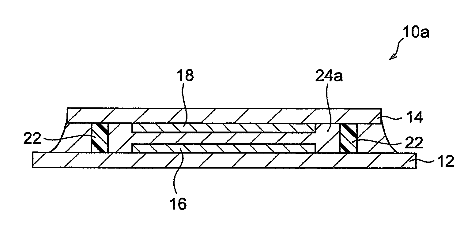
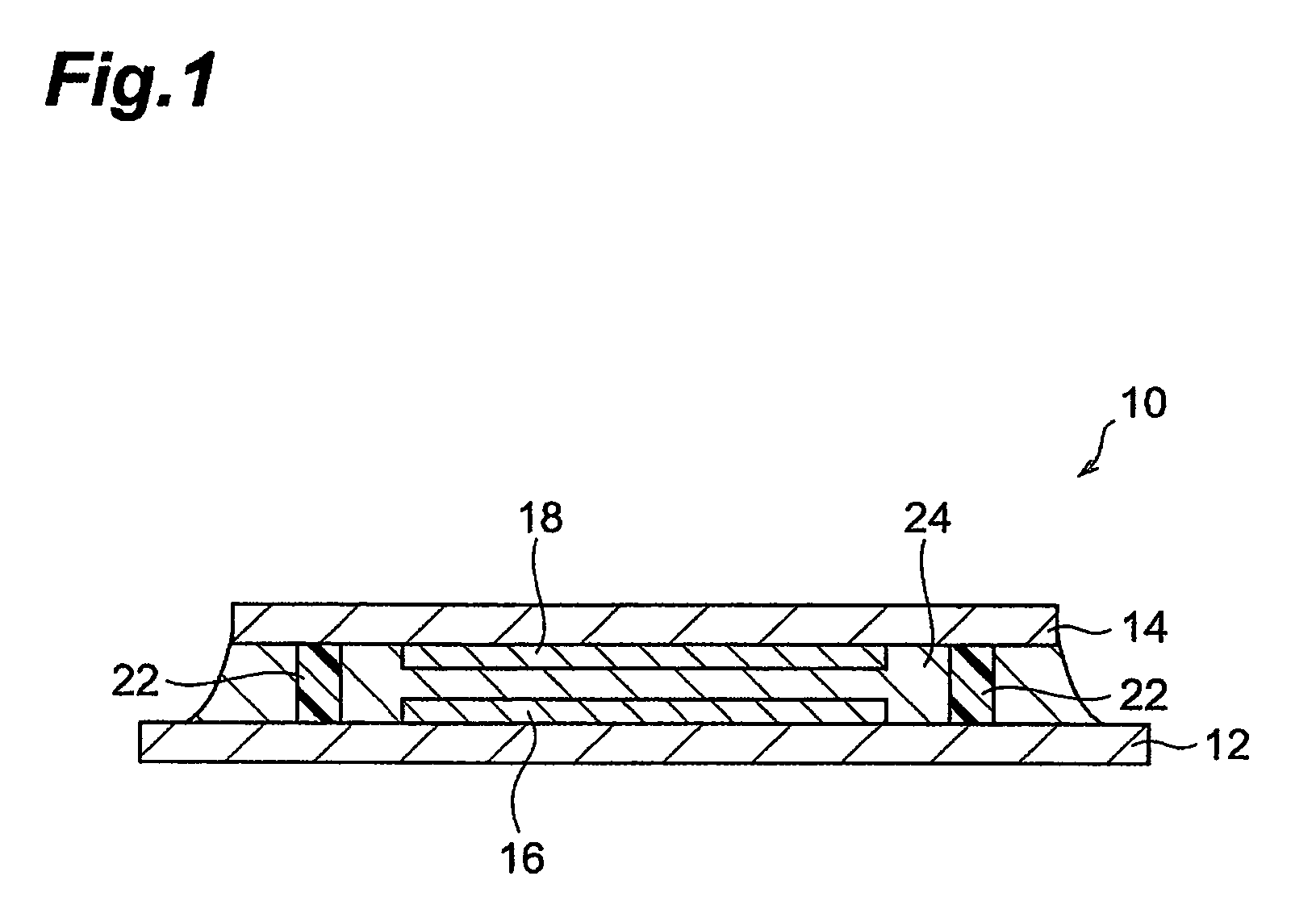
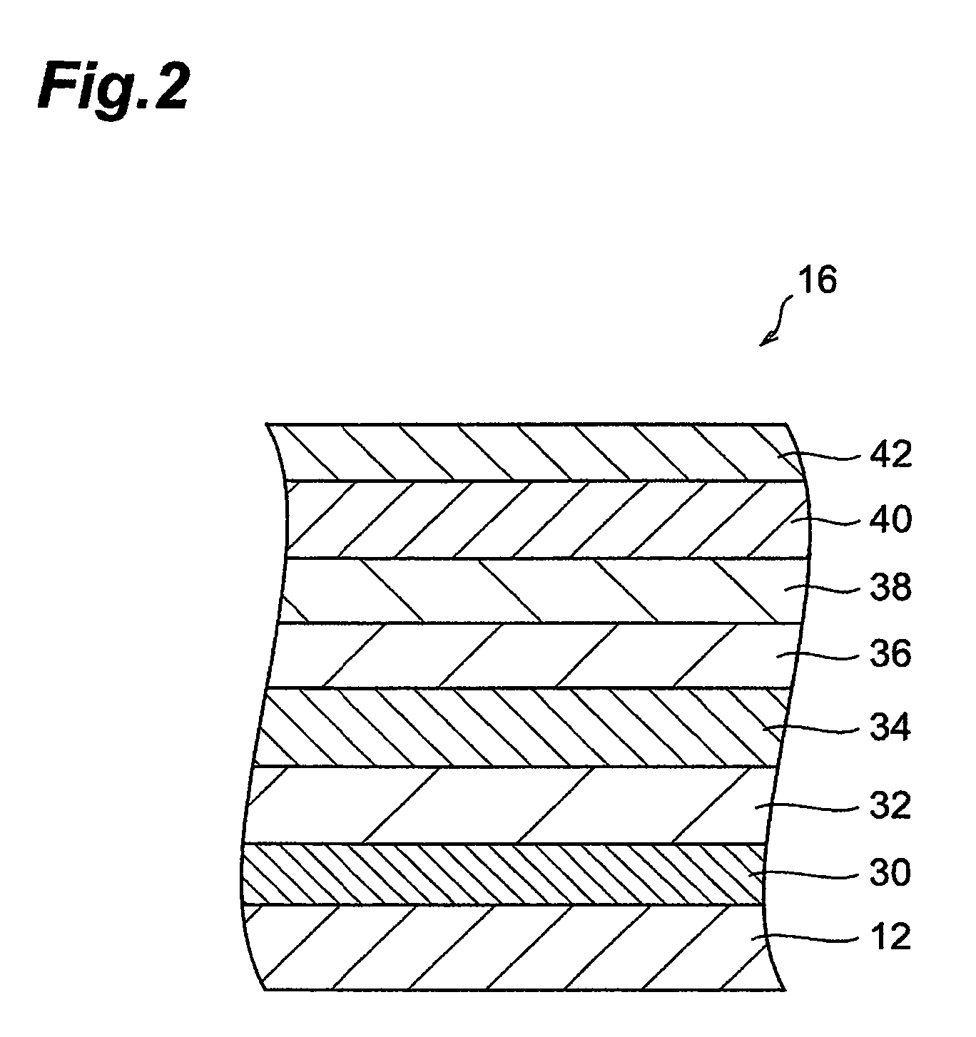
[0058]First, an organic EL device in which an EL device portion was provided on a substrate was formed. Next, a spacer portion comprising a resin was disposed around the perimeter of the EL device portion on the substrate, and then a UV cationic curing type epoxy resin (XNR5570, made by Nagase Chemtex Corporation) was dripped as a sealant onto the region surrounded by the spacer. A transparent sealing plate having a color filter portion provided thereon was then disposed on the substrate such that the EL device portion and the color filter portion faced one another, and the substrate and the sealing plate were bonded together by applying pressure thereto, whereby a panel precursor was obtained.

[0059]After that, the panel precursor obtained was irradiated from the sealing plate side with UV light (output 13,000 mJ / cm2) emitted from a high-pressure mercury lamp. The sealant was thus irradiated with UV light attenuated by the color filter portion. The UV cationic curing type epoxy resi...


PUM


Abstract

The preferable method of manufacturing the EL panel comprises a panel precursor formation step of forming a panel precursor including a substrate, a sealing plate disposed facing the substrate, an EL device (EL device portion) provided on a surface of the substrate facing the sealing plate, and a sealant comprising a curable adhesive composition filled between the substrate and the sealing plate; a first curing step of irradiating the sealant with light so as to partially cure the curable adhesive composition; and a second curing step of heating the sealant after the irradiation with the light so as to further cure the curable adhesive composition.

Description

BACKGROUND OF THE INVENTION[0001]1. Field of the Invention[0002]The present invention relates to a method of manufacturing an EL panel.[0003]2. Related Background of the Invention[0004]EL devices such as organic EL (electroluminescence), inorganic EL or the like are self-emitting light-emitting devices, and are known to have the characteristic features of high brightness and ease of making the device small and light-weight, and hence are promising for application to displays, lighting and so on. However, the light-emitting materials used in such EL devices tend to be prone to degradation due to the outside air (in particular moisture due to humidity etc.), and this has been one factor hindering making such EL devices have a long lifetime. Consequently, hitherto, to reduce contact with the outside air and thus lengthen the lifetime of EL devices, an EL panel form has often been used in which structures constituting the device are sealed between a substrate and a sealing plate.[0005]I...

Claims


Application Information

Patent Timeline
Patent Type & Authority Patents(United States)
IPC IPC(8): H01J9/00
CPCH01L51/5237H10K59/8723H10K59/8722H10K50/8428H10K50/8426
Inventor SEKI, JUNICHIAZUMA, YUKIHIRO
Owner FUTABA CORPORATION
Why Eureka
Try Eureka