Solid state imaging device including a converging structure

a technology of converging structure and imaging device, which is applied in the direction of radio frequency controlled devices, instruments, television systems, etc., can solve the problems of hardly putting all the microlenses into exactly the same shape, and the size of solid state imaging devices is even smaller, so as to improve the efficiency of focusing light, prevent light from permeating the transfer electrode, and improve the refractive index

Inactive Publication Date: 2009-02-17
FUJIFILM CORP
View PDF7 Cites 11 Cited by
  • Summary
  • Abstract
  • Description
  • Claims
  • Application Information

AI Technical Summary

Benefits of technology

[0007]In view of the foregoing, a primary object of the present invention is to provide a solid state imaging device to improve an efficiency for focusing light rays toward light receiving elements in a semiconductor substrate.
[0008]Another object of the present invention is to provide a solid state imaging device to prevent light rays from heading to transfer electrodes and avoid an occurrence of smear noise.
[0011]According to the solid state imaging device of the present invention, the covering structure that has a higher refractive index than the surrounding medium is provided inside each of the openings for the photodiodes. This configuration improves the efficiency for focusing light toward the light receiving elements. It is therefore possible to prevent light from permeating transfer electrodes, and smear noise is prevented.
[0012]Since the converging structure is appropriately adjusted in shape, refractive index, and center portion's thickness, the focusing efficiency is more improved. In accordance with the embodiment using the anti-reflection film between the converging structure and the photodiode, reflection of the incident light is prevented effectively and the focusing efficiency is even more improved.

Problems solved by technology

Unfortunately, the present-day dry etching techniques hardly put all the microlenses 109a into exactly the same shape.
Additionally, the solid state imaging devices are becoming even smaller yet hold more pixels in these days, and the photodiodes are getting smaller in dimension.
However, even these solid state imaging devices cannot provide sufficient focusing efficiency and sometimes cause smear noise that appears as a vertical whitish line on a captured image.
Insufficient focusing, however, allows some of the incident light rays to go toward the light shielding layer 105.
Another disadvantage of the Japanese Patent Laid-open Publication No. 2001-44406 is that the condensing lens above the light receiving part has a lower refractive index than the surrounding planarizing layer.
This configuration makes the light rays proceeding form a flattening, or planarizing, layer toward the condensing lens more likely to diffuse and may possibly deteriorate the focusing efficiency.
Another disadvantage of the Japanese Patent Laid-open Publication No. 2000-150845 is the formation of the well-form trench structure that extends from the microlens toward the light receiving part.
Such a trench structure is very difficult to form in modern solid state imaging devices that are so small in dimension.
As a result, voids and other defects are more likely to occur, and effective focusing of light rays on the light receiving part is hardly achieved.

Method used


Image

  • Solid state imaging device including a converging structure
  • Solid state imaging device including a converging structure
  • Solid state imaging device including a converging structure

Examples


Embodiment Construction

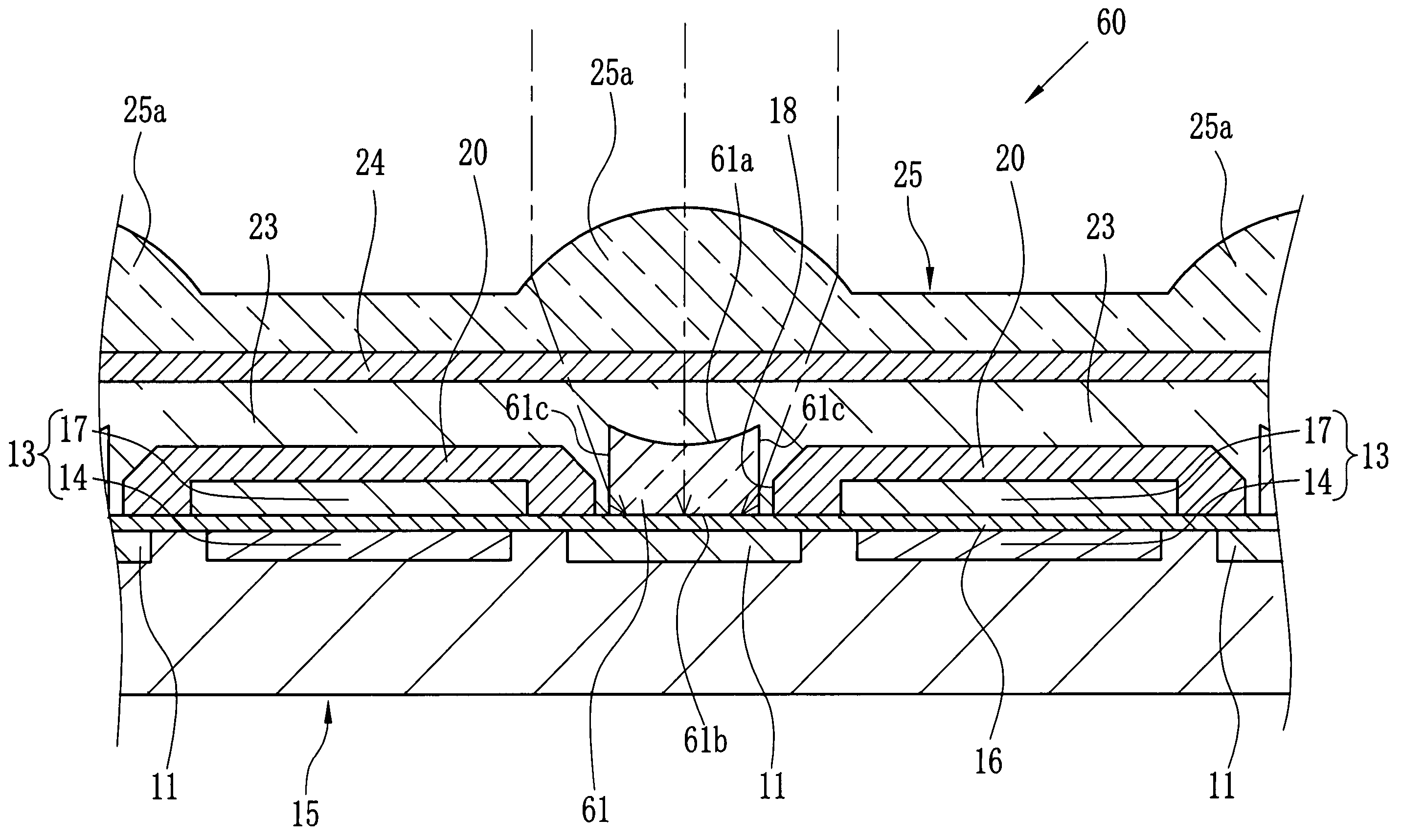
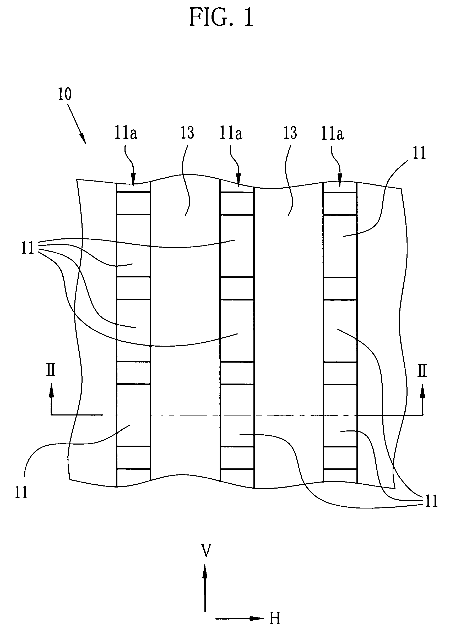
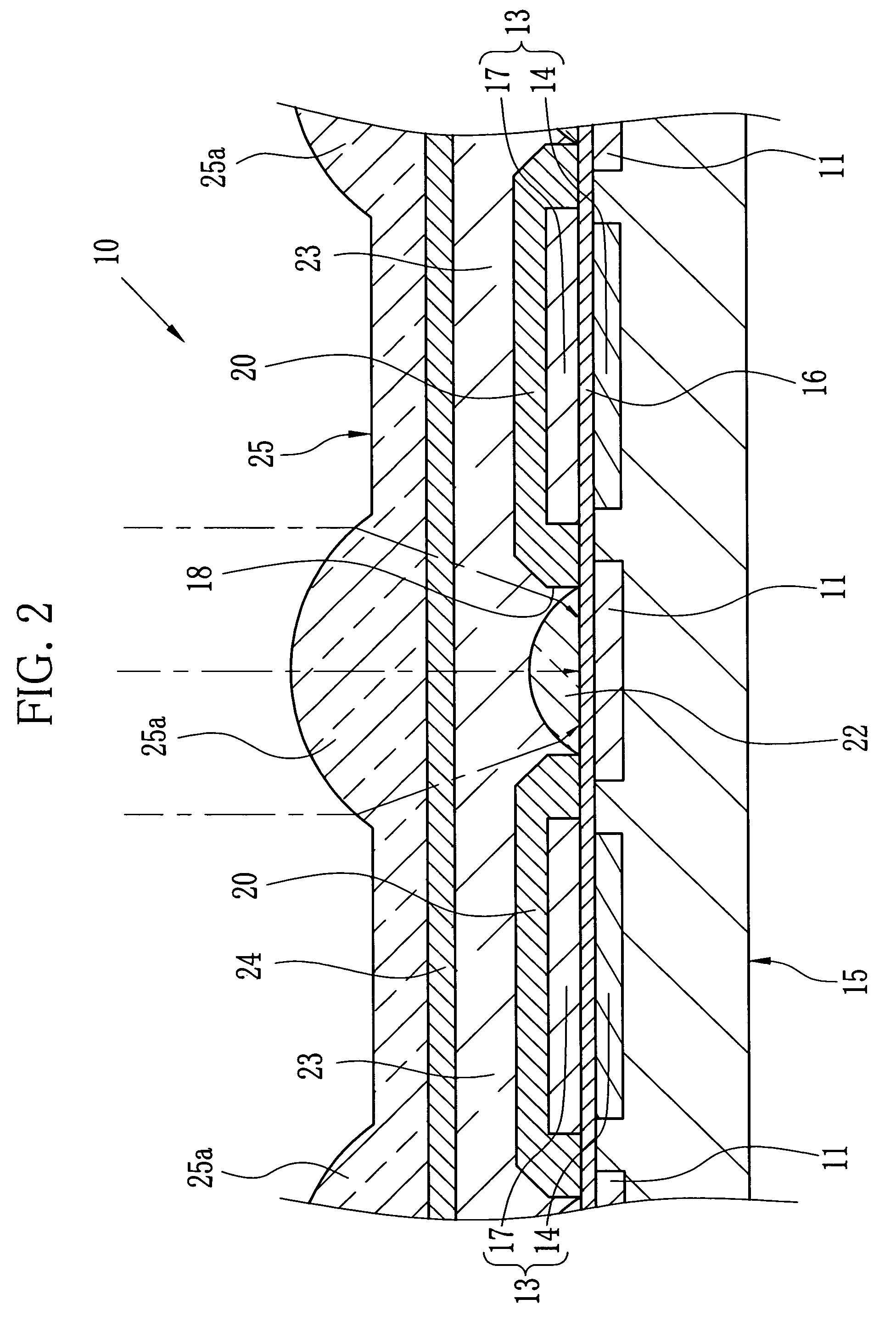
[0021]Referring to FIG. 1, a solid state imaging device such as, for example, a CCD 10 has a plurality of photodiode arrays 11a that extend in a vertical transfer direction V. Each photodiode array 11a includes a plurality of photodiodes (light receiving elements) 11 arranged at regular intervals. Formed next to the photodiode arrays 11a are vertical transfer paths 13 that also extend in the vertical transfer direction V. It is to be noted that an upper structure, such as a light shielding layer, is not illustrated in FIG. 1.

[0022]As shown in FIG. 2, the CCD 10 has a semiconductor substrate 15 on which the photodiode arrays 11a and charge transfer sections 14 are formed one after the other in a horizontal transfer direction H (see, FIG. 1). Above the charge transfer sections 14 across an insulating layer 16, transfer electrodes 17 are formed. The charge transfer section 14 and the transfer electrode 17 constitute the vertical transfer path 13 shown in FIG. 1, and vertically transfer...


PUM


Abstract

A solid state imaging device has a semiconductor substrate with photodiodes and charge transfer sections formed thereon, transfer electrodes formed on the charge transfer sections across an insulating layer, and a light shielding layer to protect the charge transfer sections from light. The light shielding layer has openings to correspond the positions of the photodiodes. Disposed above the openings of the light shielding layer are microlenses, and a converging structure such as a converging lens is provided inside each opening. Incident light rays from the microlens are focused toward the photodiode effectively by the converging lens.

Description

FIELD OF THE INVENTION[0001]The present invention relates to a solid state imaging device with excellent focusing efficiency.BACKGROUND OF THE INVENTION[0002]Recently, digital cameras are widely used which convert images, captured by a solid state imaging device such as CCD, into digital image data and store the data in recording media, such as an internal memory and a memory card. In order to facilitate focusing light rays on light receiving elements, such as photodiodes arranged in a matrix, the solid state imaging device in such digital cameras is generally equipped with microlenses located above the light receiving elements.[0003]FIG. 7 illustrates a structure in cross section of a conventional CCD. In FIG. 7, a CCD 100 includes a semiconductor substrate 102 with photodiodes 101 formed therein, a transparent insulating film 103 on a top surface of the semiconductor substrate 102, transfer electrodes 104 next to each line of the photodiodes 101, a light shielding layer 105 to cov...

Claims


Application Information

Patent Timeline
Patent Type & Authority Patents(United States)
IPC IPC(8): H01L27/00H01L27/14H01L27/148H04N5/335H04N5/359H04N5/369
CPCH01L27/14627H01L27/14818
Inventor TANI, TAKEHARU
Owner FUJIFILM CORP
Why Eureka
Try Eureka