

Solid-state imaging device, solid-state imaging device manufacturing method, electronic device, and lens array
Active Publication Date: 2011-03-31
SONY CORP
View PDF6 Cites 28 Cited by
- Summary
- Abstract
- Description
- Claims
- Application Information
AI Technical Summary
Benefits of technology
[0020]It has been found to be desirable to provide a solid-state imaging device, a solid-state imaging device manufacturing method, an electronic device, and a lens array, whereby focusing efficiency can be improved by forming a micro lens with high precision, and the image quality of an imaged image can readily be improved.
[0039]With the above configurations, the micro lenses are high in the curvature of the micro lenses in the diagonal direction (the lens thickness is thick), and accordingly, for example, can effectively focus incident light onto the light-receiving surface from the diagonal direction where smear is prevented from occurring with a CCD type. Subsequently, sensitivity can be improved along with this.
[0040]According to the above configurations, a solid-state imaging device, a solid-state imaging device manufacturing method, an electronic device, and a lens array can be provided, wherein focusing efficiency can be improved by forming micro lenses with high precision, and the image quality of an imaged image can readily be improved.
Problems solved by technology
However, in the event that a micro lens is formed by subjecting the pattern-processed lens material layer to a reflow process (in the case of the former manufacturing method), an inconvenience may be caused, such as increase in cost, difficulty in manufacturing in a stable manner, or the like.
In particular, in order to prevent adjacent micro lenses from being fused and the shapes thereof from collapsing by the reflow process, when taking various types of measures, occurrence of this inconvenience becomes prominent.
For example, increase in cost may be caused due to having to use an expensive photo mask (Japanese Unexamined Patent Application Publication No. 2007-316153), increase in the number of processes, having to invest in facilities, or the like.
Also, a product may not readily be manufactured in a stable manner due to unevenness between material lots of new materials, or unevenness between process conditions (e.g., see Japanese Unexamined Patent Application Publication Nos. 2000-206310, 2003-222705, 2007-316153, and 2007-294779).
Also, even when forming a micro lens by subjecting the lens material layer to etchback using a mask layer processed into a lens shape (in the case of the latter manufacturing method), the same inconvenience as the above may be caused.
With this manufacturing method, the effective areas of micro lenses can readily be enlarged, but distance between the micro lenses is longer in the diagonal directions of the lenses compared to the side directions, and accordingly, etchback has to be performed for a long time, which incurs deterioration in dark current or the like, and the image quality of an imaged image may deteriorate (e.g., see Japanese Unexamined Patent Application Publication No. 2007-025383 and Japanese Patent No. 4186238).
Thus, with micro lens manufacturing, it may be difficult to form micro lens with high precision, and focusing efficiency may not readily be improved.
Further, inconvenience may be caused such as increase in cost, deterioration in manufacturing efficiency, or the like.
The image quality of an imaged image may deteriorate due to the above causes.
Specifically, in the case of a CCD type, inconvenience may occur, such as deterioration in sensitivity, occurrence of smear, shading, or color mixture, or the like.
Method used
View moreImage
Smart ImageViewing Examples

Examples
first embodiment (
1. First Embodiment (Case where the curvature in the diagonal direction of OCL is higher than that in the horizontal direction at a CCD type)
second embodiment (
2. Second Embodiment (Case where the curvature in the diagonal and vertical directions of OCL is higher than that in the horizontal direction at the CCD type)
third embodiment (
3. Third Embodiment (Case where the shape of OCL is a dome-like shape at the CCD type)
Login to View More PUM
 Abstract
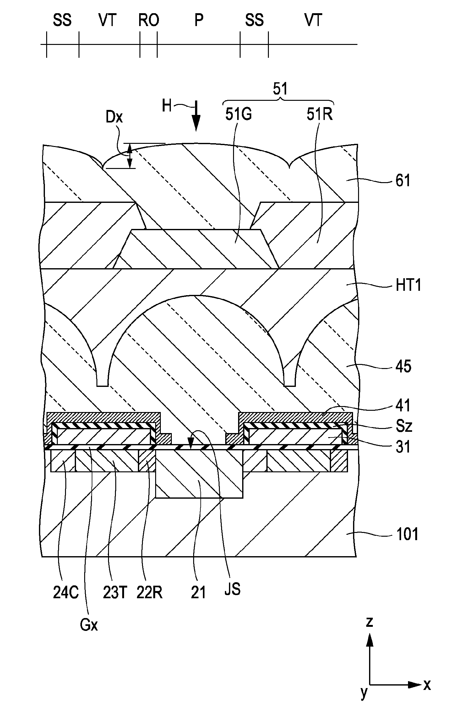
A solid-state imaging device includes: multiple micro lenses, which are disposed in each of a first direction and a second direction orthogonal to the first direction, focus the incident light into the light-receiving surface; with the multiple micro lenses of which the planar shape is a shape including a portion divided by a side extending in the first direction and a side extending in the second direction being disposed arrayed mutually adjacent to each of the first direction and the second direction; and with the multiple micro lenses being formed so that the depth of a groove between micro lenses arrayed in a third direction is deeper than the depth of a groove between micro lenses arrayed in the first direction, and also the curvature of the lens surface in the third direction is higher than the curvature of the lens surface in the first direction.
Description
BACKGROUND OF THE INVENTION[0001]1. Field of the Invention[0002]The present invention relates to a solid-state imaging device, a solid-state imaging device manufacturing method, an electronic device, and a lens array.[0003]2. Description of the Related Art[0004]Cameras such as digital video cameras and digital still cameras include solid-state imaging devices, e.g., include CMOS (Complementary Metal Oxide Semiconductor) image sensors or CCD (Charge Coupled Device) image sensors as a solid-state imaging device.[0005]With solid-state imaging devices, an imaging region where multiple pixels are formed is provided to the surface of the semiconductor substrate. With this imaging region, multiple photoelectric conversion units which receive light according to a subject image, and generate signal charge by subjecting the received light thereof to photoelectric conversion, are formed so as to correspond to the multiple pixels thereof. For example, photodiodes are formed as the photoelectric...
Claims
Login to View More Application Information
Patent Timeline
 IPC IPC(8): H01L27/146G02B27/12
CPCG02B3/0056H01L27/14609H01L27/1464H01L27/14643H01L27/14627H01L27/146H01L27/14625H04N1/19526H04N1/195H01L27/148H01L27/14685H01L27/14612H04N25/67H04N25/616H04N25/745
InventorOGINO, AKIKOOTSUKA, YOICHI
OwnerSONY CORP