Submount and its manufacturing method

a manufacturing method and submount technology, applied in the direction of semiconductor/solid-state device details, radiation control devices, lighting support devices, etc., can solve the problems of increased product price, limited density of led elements, etc., to achieve rational production, improve heat radiating properties, and effectively focus light

Active Publication Date: 2009-09-03
HITACHI KYOWA ENG
View PDF5 Cites 34 Cited by
  • Summary
  • Abstract
  • Description
  • Claims
  • Application Information

AI Technical Summary

Benefits of technology

[0013](3) Moreover, the metallized joint of the first substrate and the glass of the second substrate are jointed by anodic bonding, which makes it possible to join the first substrate and the second substrate together in a wafer state, and can contribute to rationalization of production of the submounts, as well as providing inexpensive submounts.
[0014]As described above, according to the present invention, optical devices represented by, for example, LEDs can be mounted in a high density, and it is possible to provide a submount for LEDs which can effectively focus light, has an improved heat radiating property, and is inexpensive, and an optical module in which optical devices are mounted on the submount. When LEDs generating red, green, and blue light components are combined, it is possible to synthesize the light components to generate white light or to control power of each optical device to change the color tone of light.
[0015]Moreover, it is possible to manufacture a submount by anodic bonding by using a substrate formed of glass or by jointing glass and silicon as a material of a substrate on which a light reflecting film has been formed. The anodic bonding is a technique suitable for joining wafers or plate-shaped objects and can reduce the manufacturing cost to provide an inexpensive submount.

Problems solved by technology

Further, in the case of LED elements molded by use of a resin or the like according to the related art, there is a limitation in densely arranging LED elements.
However, if lenses are used for every LED element, the cost results in a rise in product price and supporting members are needed to fix the lenses over the LED elements.

Method used


Image

  • Submount and its manufacturing method
  • Submount and its manufacturing method
  • Submount and its manufacturing method

Examples


first embodiment

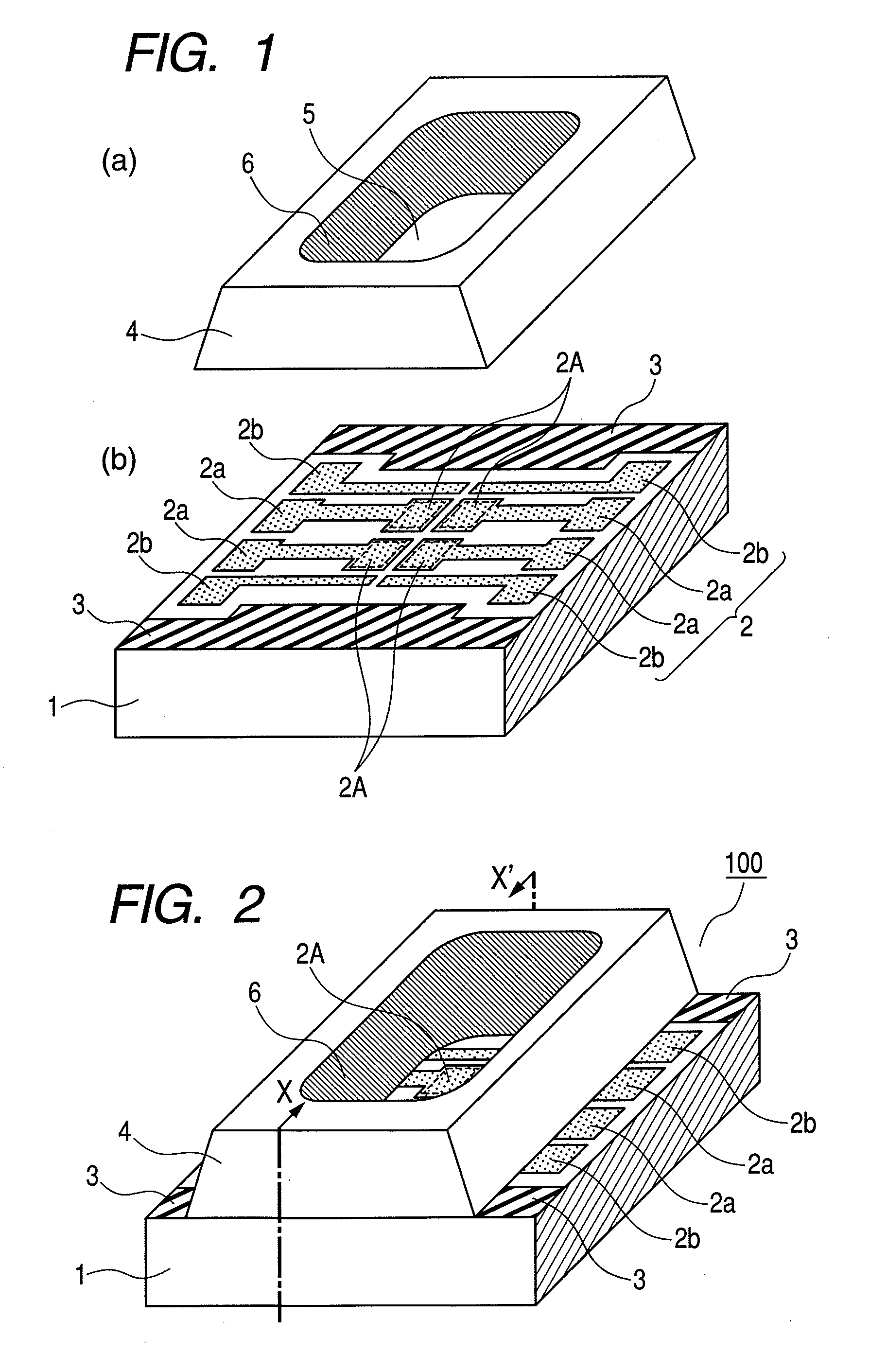
[0055]A first embodiment of the present invention will be described with reference to FIGS. 1 to 6.

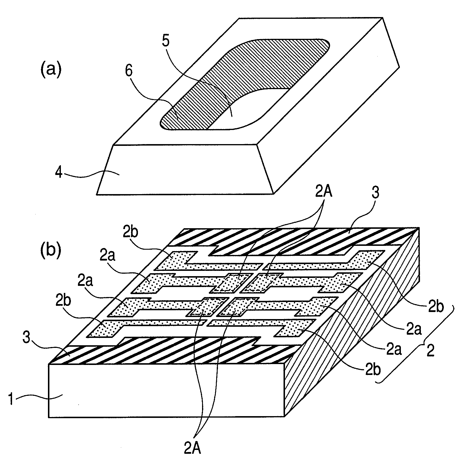
[0056]FIG. 1 shows an exploded view of minimum configuration unit portions of a submount according to the present invention for showing an image of a completed product after substrates have been processed, jointed, and cut. FIG. 1(a) shows a perspective view of a second substrate 4 before being jointed, and FIG. 1(b) shows a perspective view of a first substrate 1 before being jointed. Reference numeral 5 represents a through hole and reference numeral 6 represents a reflective film provided on the wall of the through hole.

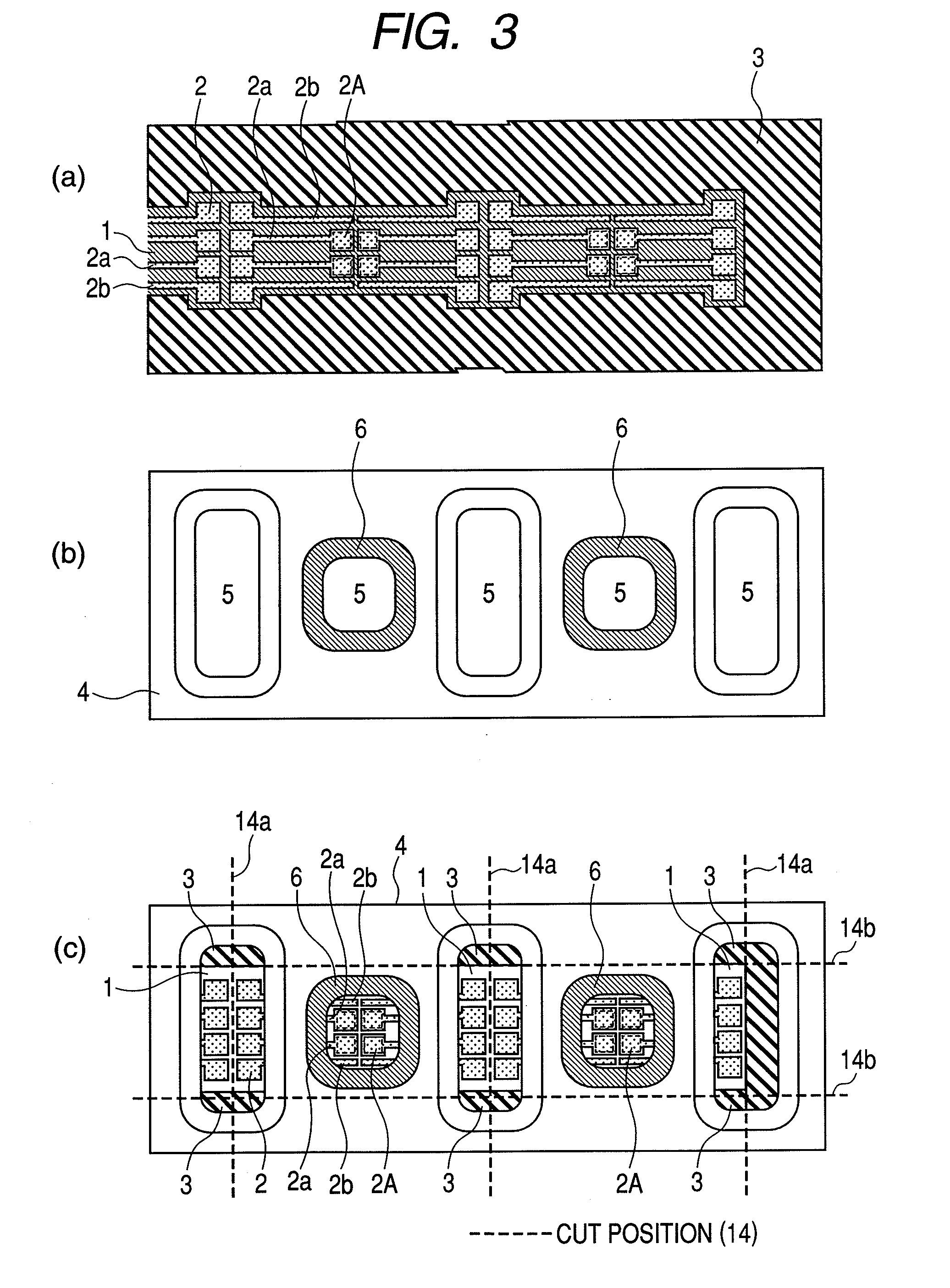
[0057]FIG. 2 is a perspective view of a submount 100 after a first substrate 1 and a second substrate 4 are aligned with each other and both substrates 1 and 4 are jointed. FIGS. 3(a) and 3(b) are top views illustrating the states of the substrates (wafers) 1 and 4 before aligning, respectively. FIG. 3(c) is a top view of the substrates after the substrates 1 and 4 a...

second embodiment

[0089]A second embodiment of the present invention will be described with reference to FIG. 7 which is an exploded view of a submount 100. Even in this embodiment, minimum configuration units of a submount are taken out and shown. In other words, FIG. 7(a) shows a second substrate 4 before joining, FIG. 7(b) shows a first substrate 1 before joining, and in an actual manufacturing process, it is possible to manufacture a batch of submounts by processing, joining, and cutting wafers or plate-shaped first and second substrates 1 and 4, similar to the first embodiment. This is similar even in the following embodiments.

[0090]As shown in FIG. 7(b), a resist pattern (not shown), in which a portion (which is in a semicircular shape as an image cut at the center of the hole in the drawing) to become a hole of a through hole 10 is hollowed, is formed at the outer circumference of a forming region of the optical device mounting parts 2A of the first substrate 1 formed of silicon carbide cerami...

third embodiment

[0100]A third embodiment of the present invention will be described with reference to FIGS. 11 and 12. The manufacturing of the first substrate 1 is similar to that in the second embodiment, FIG. 11 corresponds to FIG. 9, and FIG. 12 is a cross sectional view taken along the line Z-Z′ of FIG. 11 and corresponds to FIG. 10.

[0101]As shown in FIG. 12, silicon 11 and Pyrex glass 12 are bonded to each other in advance by a method such as anodic bonding, which is used for the second substrate 4. In forming the through hole 5 in the silicon 11, it is possible to form a sloping surface of the wall of the hole as shown in the drawing by using a wet etching technique which is being used for manufacturing semiconductor devices.

[0102]First, a mask is formed on a silicon wafer in which the (100) plane becomes a surface by a photolithographic technique. The mask is made so that an etched part becomes an opening. If this is soaked in an etching solution of an appropriate concentration, an etching ...


PUM

PropertyMeasurementUnit
thicknessaaaaaaaaaa
thicknessaaaaaaaaaa
thicknessaaaaaaaaaa

Abstract

Submounts for mounting optical devices which have an excellent heat radiating property and can be formed in a wafer state in batch are provided.A metallized electrode including optical device mounting parts and wiring parts is formed on a surface of a first substrate containing an insulating material as a main component, a through hole is formed in a glass substrate serving as a second substrate, the optical device mounting parts of the first substrate are aligned to be located inside the through hole of the second substrate, and the first substrate and the second substrate are joined together by use of a method such as anodic bonding.

Description

FIELD OF THE INVENTION[0001]The present invention relates to a structure of a submount and a manufacturing method thereof, and in particular, to a submount appropriate to mount a surface-emitting type of optical device such as a semiconductor light-emitting device thereon and to effectively focus light in a light emitting direction of the device, an optical module in which an optical device is mounted on a submount, and a manufacturing method thereof.BACKGROUND OF THE INVENTION[0002]With respect to a surface-emitting type of optical devices, in particular, LED (Light Emitting Diode), recently, the characteristics thereof have been improved, and expectations for usage expansion are high. According to the related art, an LED is mounted in a plastic case and a micro lens or the like is disposed in a light path to focus light. Alternatively, all of an LED and a substrate having the LED mounted thereon are molded in a transparent resin and the surface of the resin is shaped into a smooth...

Claims


Application Information

Patent Timeline
Patent Type & Authority Applications(United States)
IPC IPC(8): F21V19/00B32B38/10H01L33/60H01L33/62H01L33/64
CPCH01L25/0753H01L33/46H01L33/486H01L33/62H01L33/641H01L2224/48091H01L2224/48227H01L2924/10253H01L2924/09701H01L2224/73265H01L2924/00014H01L2924/00
Inventor HATA, SHOHEISAKAMOTO, EIJIMATSUSHIMA, NAOKITAKEMORI, HIDEAKISEKI, MASATOSHI
Owner HITACHI KYOWA ENG
Why Eureka
Try Eureka