Display device having display surfaces with polarizing plates

a display device and polarizing plate technology, applied in the field of display devices, can solve the problems of reducing the external light reflection in the electrode described above, affecting the display effect, so as to reduce the reflection and improve the contrast

Inactive Publication Date: 2009-02-24
SEMICON ENERGY LAB CO LTD
View PDF30 Cites 23 Cited by
  • Summary
  • Abstract
  • Description
  • Claims
  • Application Information

AI Technical Summary

Benefits of technology

[0008]It is an object of the present invention to provide a display device which has a plurality of display surfaces and which further achieves lightweight and thin. Then, problems of a display device having such a new structure will be solved.
[0009]A display device in which light is emitted from both sides of a light emitting element (referred to as a dual emission display device) will be provided in view of the above problems. A dual emission display device has a structure technically different from the structure of a cellular phone in which two-screen display is performed by using display areas respectively having light emitting elements stacked together. That is a structure in which light emission from one light emitting element can be recognized from the side that a semiconductor element is provided and also from the opposite side. Thus, an electronic device having a dual emission display device can be made thin and lightweight.
[0011]As thus described, another problem in dual emission display device has been arisen. Hence, it is an object of the invention to provide a dual emission display device which can perform pure black display and can achieve high contrast.
[0017]Further, a polarizing plate or a circularly polarizing plate may be provided with an anti-reflective film. For example, anti-glare treatment can be performed by diffusing reflected light in the depression / projection of the surface, thereby reducing reflection. Alternatively, anti-reflection treatment may be performed on a polarizing plate or a circularly polarizing plate by heat-treatment. Thereafter, hard coat treatment may preferably be done for the protection from external shock.
[0018]As described above, the problem of black display in a new structure of a dual emission display device in which light is released from both sides of a light emitting element can be solved. In addition, the contrast can be improved

Problems solved by technology

In consequence, the problem of external light reflection in an electrode described above can be reduced; however, another problem of difficulties in displaying black color (black display) arises.
The problem arises since the both electrodes are transparent and in case of black display, in OFF state where no image is displayed, the other side can be seen therethrough.
As thus described, another problem in dual emission display device has been arisen.

Method used


Image

  • Display device having display surfaces with polarizing plates
  • Display device having display surfaces with polarizing plates
  • Display device having display surfaces with polarizing plates

Examples


embodiment modes

[0031]Embodiment modes of the present invention will be described below with reference to the accompanying drawings. Note that in all figures for describing the embodiment modes, the same reference numerals denote the same parts or parts having the same function, and the explanation will not be repeated.

embodiment mode 1

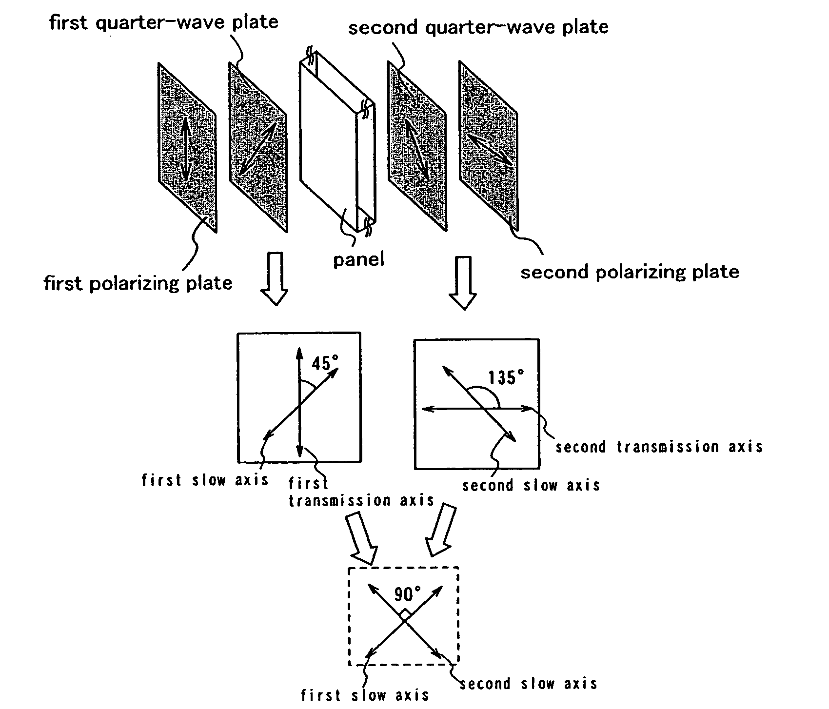
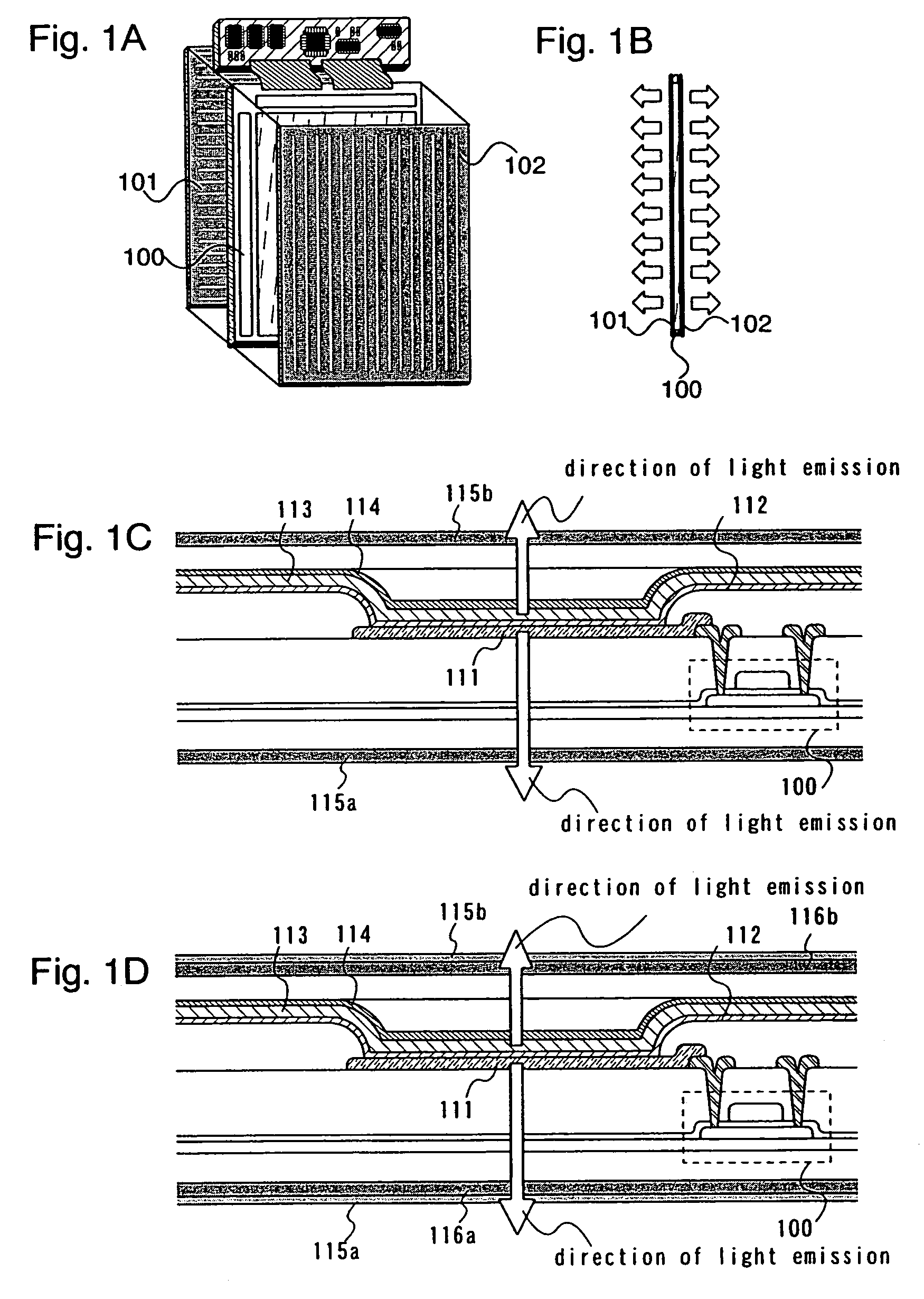
[0032]In this embodiment mode, a case where a polarizing plate or a circularly polarizing plate is provided in a dual emission display device will be described.

[0033]A general view of a dual emission display device is shown FIG. 1A. A first polarizing plate 101 is disposed on a panel 100 of a dual emission display device, and a second polarizing plate 102 is arranged as crossed nicols, that is the axes of the first and the second polarizing plates are at 90° with the first polarizing plate.

[0034]Hereupon, the axes of polarizing plates may have angular deviation from crossed nicols configuration, and the angular deviation may be ±45° or less, preferably, ±30° or less, and further preferably, ±10° or less, and still further preferably, ±5° or less. When the angular deviation from crossed nicols configuration is ±45° or less, the transmitted light is reduced by 50% compared with the transmitted light under parallel nicols configuration as is shown in Embodiment 2. Further, in the case ...

embodiment mode 2

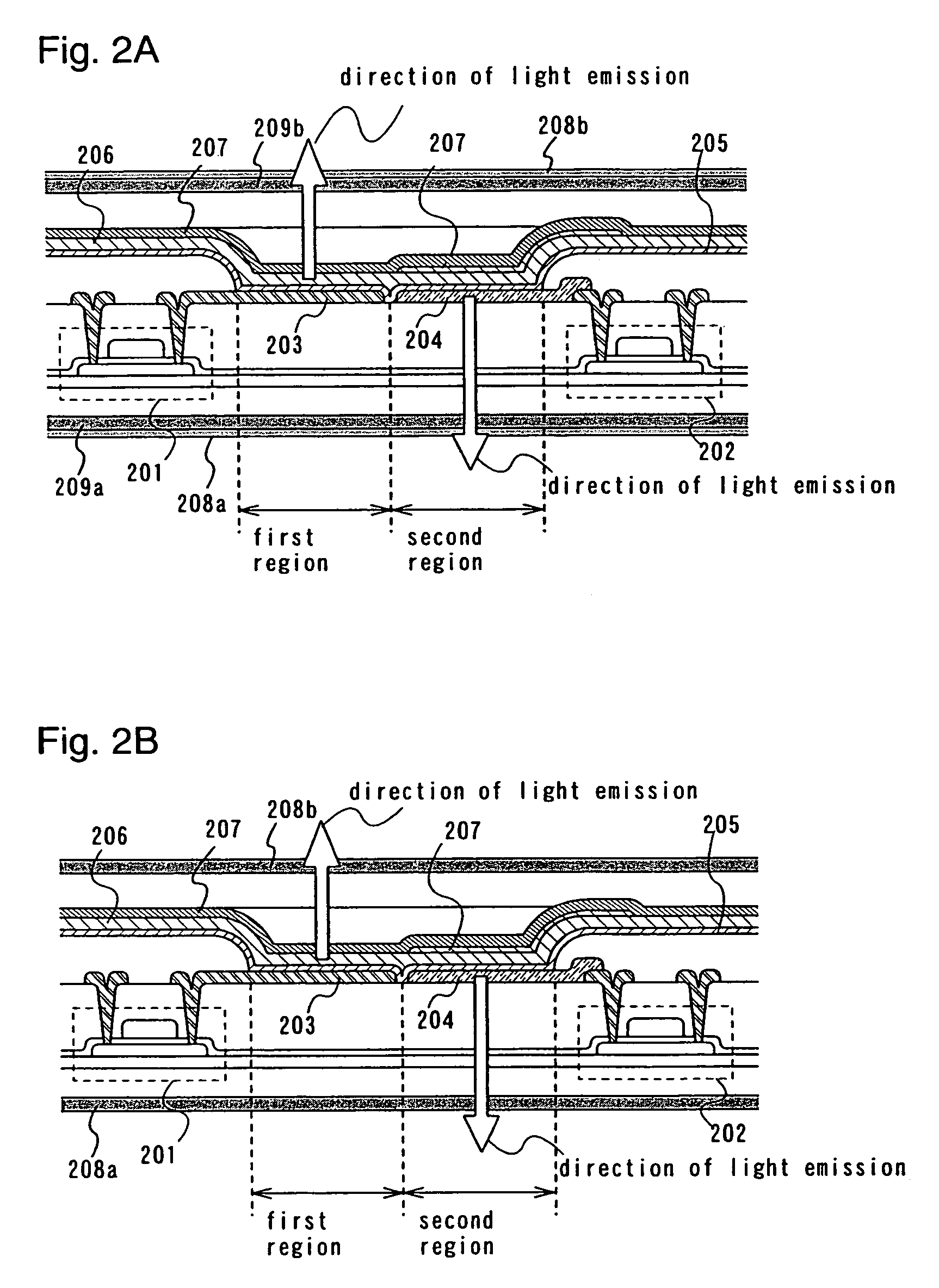
[0055]In this embodiment mode, a structure of a dual emission display device different from that of FIGS. 1A to 1D in the case where a circularly polarizing plate or a polarizing plate is provided will be described.

[0056]As for the dual emission display device different from the one in FIG. 1C, light is emitted from the second electrode side in a first area, and light is emitted from the first electrode side in a second area. Accordingly, a plurality of light emitting elements and a plurality of driver TFTs are provided in one pixel; the first electrode electrically connected to the first light emitting element is opaque and the second electrode opposed to the first electrode is transparent. The first electrode electrically connected to the second light emitting element is transparent, and the second electrode opposed to the first electrode is opaque. A film containing metal or colored resin may be formed on the transparent / translucent electrode so as to obtain opacity.

[0057]In this...


PUM


Abstract

As for the dual emission display device, since light is emitted to the opposite directions from a light emitting element, the both electrodes provided opposite to the light emitting element are transparent / translucent. Accordingly, difficulty in black display is created, and thus, the contrast would be reduced. That results from that the back of the display device can be seen through in black display, that is in the OFF state, since the both electrodes have transparency. Addressing the difficulty in black display with respect to an electronic device and the like including a dual emission display device achieving reduction in the thickness and light weighting, pure black display is performed by providing the dual emission display device part with a polarizing plate or a circularly polarizing plate. Further, the contrast can be improved.

Description

BACKGROUND OF THE INVENTION[0001]1. Field of the Invention[0002]The present invention relates to a display device having a polarizing plate or a circularly polarizing plate. The present invention particularly relates to a display device in which light emitting elements are arranged in matrix and light is emitted from both sides of the light emitting element.[0003]2. Description of the Related Art[0004]A polarizing plate or a circularly polarizing plate is used for a conventional organic EL panel having an organic EL element (For example, Reference 1: Japanese Patent No. 2761453). Such an optical component is provided since external light is reflected in an electrode formed in a display area and that reduces the visibility of an image. Particularly in a state where no image is displayed, an electrode serves as a mirror surface, and the background could be reflected in the electrode. Further, even in a state where an image is displayed, problems such as reduction in contrast or diffic...

Claims


Application Information

Patent Timeline
Patent Type & Authority Patents(United States)
IPC IPC(8): H01J1/62G09F9/00H05B33/02G09F9/40G09G3/00H01J63/04H01L27/15H01L27/32H01L51/10H01L51/50H01L51/52H05B33/12H05B33/14H05B33/22
CPCH01L27/3267H01L51/5281H01L2251/5323H10K59/128H10K2102/3031H10K59/8791H10K50/868G02B5/201G02F1/133528H10K50/86
Inventor YAMAZAKI, SHUNPEIHIRAKATA, YOSHIHARUISHITANI, TETSUJI
Owner SEMICON ENERGY LAB CO LTD
Why Eureka
Try Eureka