Semiconductor memory

a technology of memory and semiconductors, applied in the direction of transistors, solid-state devices, instruments, etc., can solve the problems of increasing power consumption, difficult to lower power consumption, increasing power consumption, etc., and achieve the improvement of the performance of each transistor, the improvement of various performance of the sram, and the increase of surplus leak current

Inactive Publication Date: 2009-03-03
RENESAS ELECTRONICS CORP
View PDF13 Cites 121 Cited by
  • Summary
  • Abstract
  • Description
  • Claims
  • Application Information

AI Technical Summary

Benefits of technology

[0009]However, when a voltage of about 0.5 V or more at room temperature or of about 0.2 V or more at high temperatures is loaded to a back gate of the bulk CMOS transistor, a large junction current flows at a PN junction of the transistor, which disadvantageously results in increase of power consumption. For the reason described above, in the first and second conventional examples, increase of power consumption does not occur in a circuit operating with a power voltage of 0.2 V or below. In circuits operating at a voltage higher than the value described above, however, the power consumption increases due to the junction current, which disadvantageously makes it difficult to lower power consumption. Further the third conventional example discloses the configuration in which a threshold voltage (Vth) is controlled by using a transistor having the SOI structure. In the SOI structure, by controlling a voltage in a lower layer of the buried oxide film, an unnecessary increase in current in a transistor is suppressed and Vth of the transistor can be controlled, so that a power voltage for a SRAM can be lowered by suppressing an increase in power consumption. With this configuration, however, Vth's in the driver transistor and transfer transistor drop simultaneously in association with activation of a word line. Consequently, Vth in the driver transistor connected to a storage node storing therein “H” data becomes lower, which disadvantageously spoils operational stability of the SRAM. Further capacities of back gates of the transfer transistor and the driver transistor are added to a capacity of the word line. Therefore, a parasitic capacity of the word line increases, which disadvantageously lowers the operating speed.
[0010]By forming a SRAM memory cell with SOI transistors and properly controlling an electric potential in a lower well layer of a buried Oxide (BOX) layer of each transistor to change a current flowing in each transistor, it becomes possible to improve various performances of the SRAM. Since the well layer is electrically insulated by the BOX layer from the SOI layer with transistors provided thereon, an increase in surplus leak current never occurs. When well contact is provided properly, also the memory cell area does not increase. Further, when powers corresponding to two different voltages are selectively loaded to a specified node in a memory to change a current flowing therein, performance of each transistor can be improved. In addition, a load to the word line does not increase, so that the operating speed is not lowered.

Problems solved by technology

However, when a voltage of about 0.5 V or more at room temperature or of about 0.2 V or more at high temperatures is loaded to a back gate of the bulk CMOS transistor, a large junction current flows at a PN junction of the transistor, which disadvantageously results in increase of power consumption.
In circuits operating at a voltage higher than the value described above, however, the power consumption increases due to the junction current, which disadvantageously makes it difficult to lower power consumption.
Consequently, Vth in the driver transistor connected to a storage node storing therein “H” data becomes lower, which disadvantageously spoils operational stability of the SRAM.
Therefore, a parasitic capacity of the word line increases, which disadvantageously lowers the operating speed.

Method used


Image

  • Semiconductor memory
  • Semiconductor memory
  • Semiconductor memory

Examples


embodiment 1

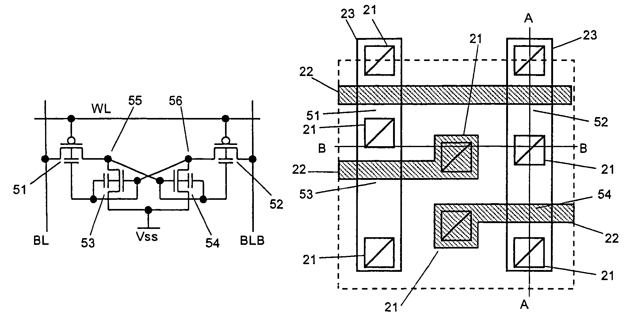
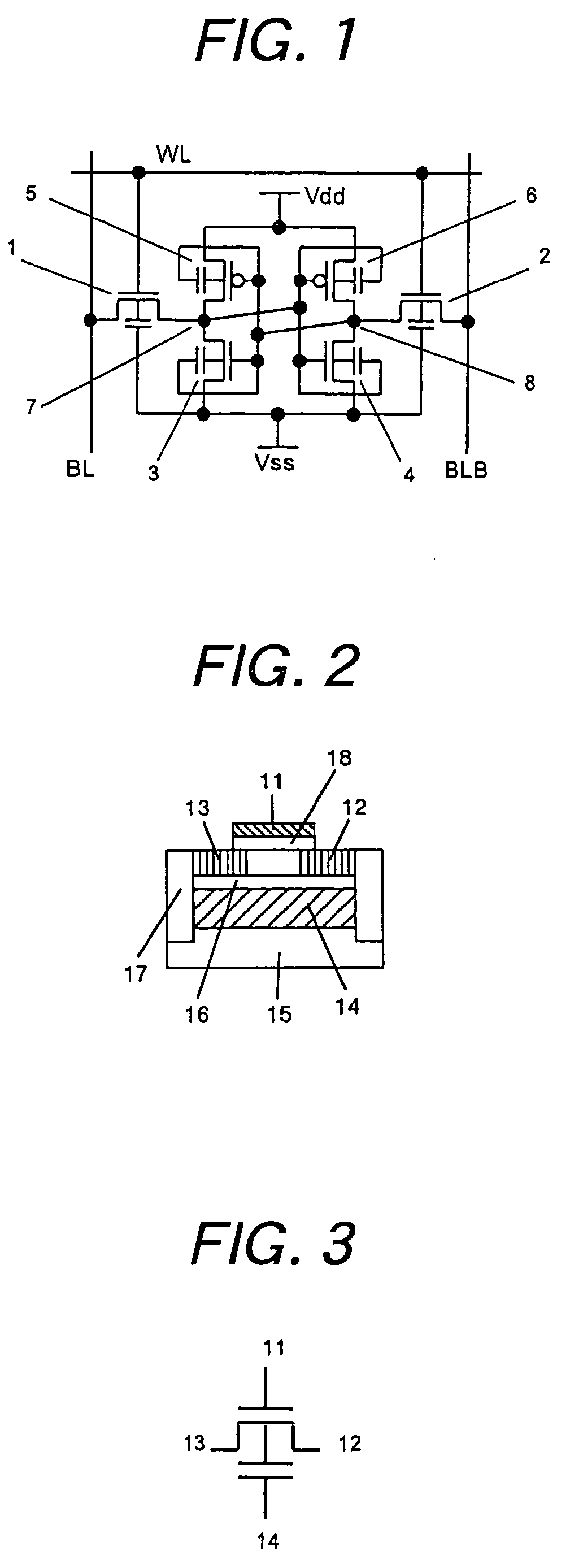
[0047]FIG. 1 is a circuit diagram showing a SRAM memory cell according to the present invention. In FIG. 1, symbols BL and BLB each indicate a bit line, WL indicates a word line, Vdd indicates a power line, and Vss indicates a ground potential line. Further reference numerals 1 and 2 each indicate a transfer transistor for access to a memory cell, 3 and 4 each indicate a driver transistor for driving a storage node for maintaining therein data for the memory cell, 5 and 6 each indicate a load transistor for supplying an electric charge for maintaining data in the memory cell, and 7 and 8 each indicate a storage node for storing data. For instance, Vdd is at an electric potential of 1.2 V, and the ground potential line Vss is at an electric potential of 0 V. FIG. 2 is a general block diagram showing a cross section of a transistor used in the circuit shown in FIG. 1. In FIG. 2, reference numeral 11 indicates a gate, 12 a drain, 13 a source, 14 a well layer under a BOX layer, 15 a sup...

embodiment 2

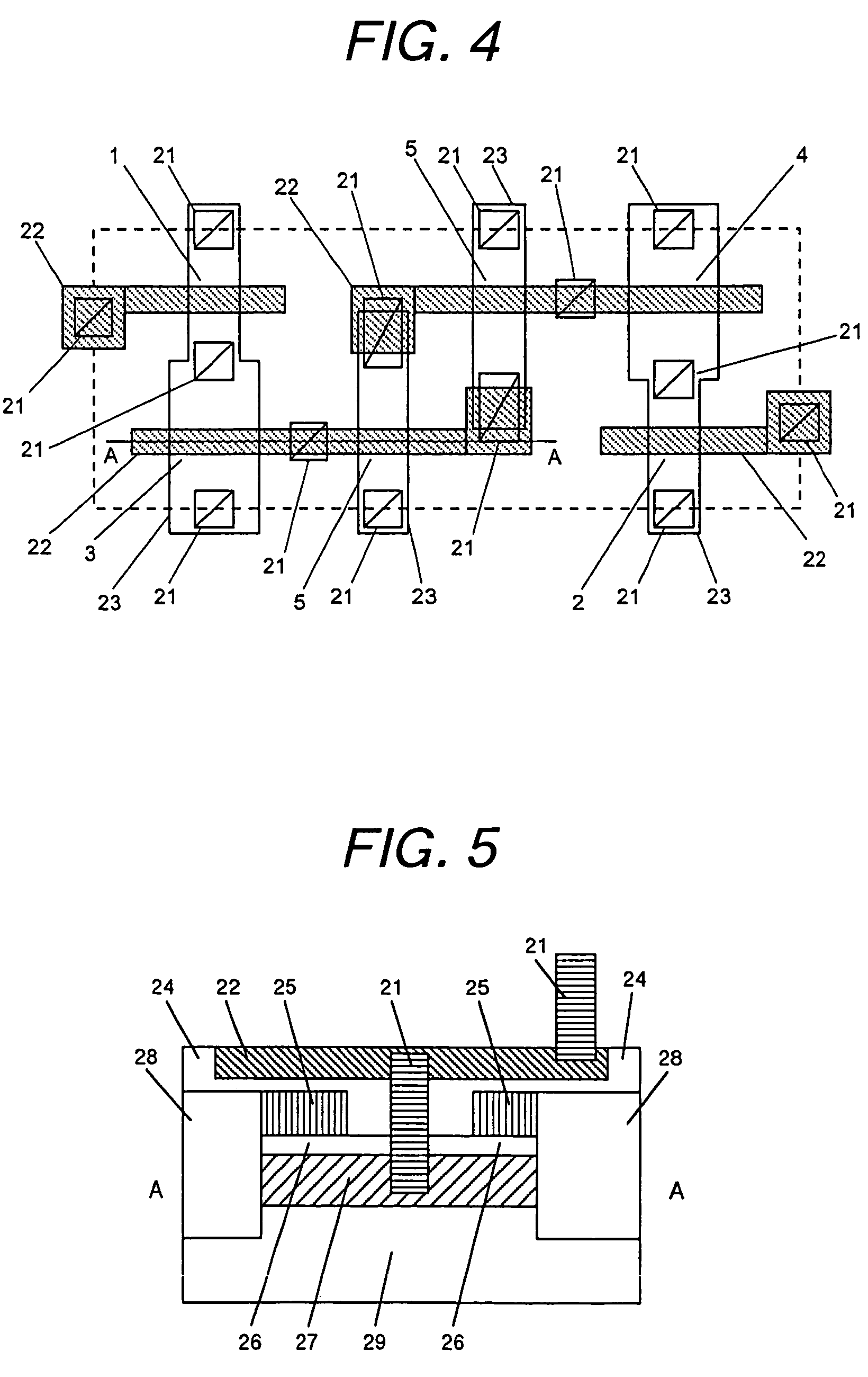
[0055]FIG. 7 shows layout of a SRAM memory cell according to the present invention. In descriptions of the following embodiments, the same reference numerals are used for the same components as those in Embodiment 1, and a description is made only of different components. The circuit configuration of this memory cell at the transistor level is the same as that shown in FIG. 1. The layout of the memory cell shown in FIG. 7 is different from that shown in FIG. 4 only in that a back gate contact for the driver transistor as well as for the load transistor is formed below a contact for connecting the gate node to the metal layer. With this configuration, the contact formed between a driver transistor and a load transistor in the conventional technology is not necessary, so that an area of the memory cell can be reduced. In particular, when a memory cell is formed of a bulk CMOS transistor, it is necessary to separate a well for a driver transistor from that for a load transistor, so tha...

embodiment 3

[0057]FIG. 9 shows layout of a SRAM memory cell according to the present invention. A circuit diagram of the memory cell shown in FIG. 9 at the transistor level is the same as that shown in FIG. 1. The memory cell shown in FIG. 9 is different from that shown in FIG. 1 only in that a gate width (W-size) of the driver transistor is the same as that of the transfer transistor. In the SRAM memory cell, as described in Embodiment 1, it is generally necessary, for the purpose of preventing an electric potential of a storage node at the “L” level from rising, that conductance of the driver transistor is larger than that of the transfer transistor. In a memory cell using a bulk CMOS transistor, the conductance is generally adjusted by controlling the W-size. The W-size of the driver transistor is set to a value about 1.5 times larger as compared to that of the transfer transistor. In this embodiment, the conductance when a back gate of the driver transistor is connected to the gate and the ...


PUM


Abstract

A SRAM memory is composed of FD-SOI transistors, and performance of the memory cell is improved by controlling an electric potential of a layer under a buried oxide film of a SOI transistor constituting a driver transistor. Performance of the SRAM circuit in the low power voltage state is improved. In the SRAM memory cell composed of the FD-SOI transistor, an electric potential of a well under a BOX layer is controlled to control a threshold voltage Vth, thereby increasing a current. Thus, the operations of the memory cell can be stabilized.

Description

CLAIM OF PRIORIRY[0001]The present application claims priority from Japanese application JP 2004-176669, filed on Jun. 15, 2004, the contents of which is hereby incorporated by reference into this application.BACKGROUND OF THE INVENTION[0002]1. Field of the Invention[0003]The present invention relates to a semiconductor integrated circuit formed with static memory (SRAM) circuits integrated on a semiconductor chip. More specifically, this invention relates to circuit configuration allowing for reduction of an operating voltage for a SRAM integrated circuit device.[0004]2. Description of the Related Art[0005]FIG. 33 shows a conventional type of a SRAM memory cell circuit. Symbols BL and BLB each indicates a bit line, WL a word line, Vdd a power line, and Vss a ground potential line. Further, reference numerals 111 and 112 denote a transfer transistor for access to a memory cell, 113 and 114 a driver transistor for driving a memory node for maintaining therein data for the memory cell...

Claims


Application Information

Patent Timeline
Patent Type & Authority Patents(United States)
IPC IPC(8): H01L27/01G11C11/00H01L27/11H01L27/12H01L31/0392G11C11/412H01L21/8244H01L27/108
CPCG11C11/412H01L21/84H01L27/11H01L27/1203H01L27/108Y10S257/903H10B12/00H10B10/00
Inventor YAMAOKA, MASANAOOSADA, KENICHIITOH, KIYOOKAWAHARA, TAKAYUKI
Owner RENESAS ELECTRONICS CORP
Why Eureka
Try Eureka