
Plasma display panel provided with alignment marks having similar pattern than electrodes and method of manufacturing the same

a technology of alignment marks and display panels, which is applied in the manufacture of electrode systems, electric discharge tubes/lamps, instruments, etc., can solve the problems of increasing process time, complicated and expensive photolighography techniques, and time-consuming, and achieves less processing time, less expensive, and less complicated effects

Inactive Publication Date: 2009-03-03
SAMSUNG SDI CO LTD
View PDF35 Cites 5 Cited by
  • Summary
  • Abstract
  • Description
  • Claims
  • Application Information

AI Technical Summary

Benefits of technology

[0013]It is also an object of the present invention to provide an improved technique of making a PDP that is less complicated, requires less processing time, and less inexpensive.

Problems solved by technology

Since the photolithography technique requires photoresist coating, photoresist patterning and then an etching process, the photolighography technique is very time consuming, is complicated and is expensive.
Therefore, the ITO material applied to the non-display region is removed by laser ablation, resulting in an increase the process time.

Method used


Image

  • Plasma display panel provided with alignment marks having similar pattern than electrodes and method of manufacturing the same
  • Plasma display panel provided with alignment marks having similar pattern than electrodes and method of manufacturing the same
  • Plasma display panel provided with alignment marks having similar pattern than electrodes and method of manufacturing the same

Examples


Embodiment Construction

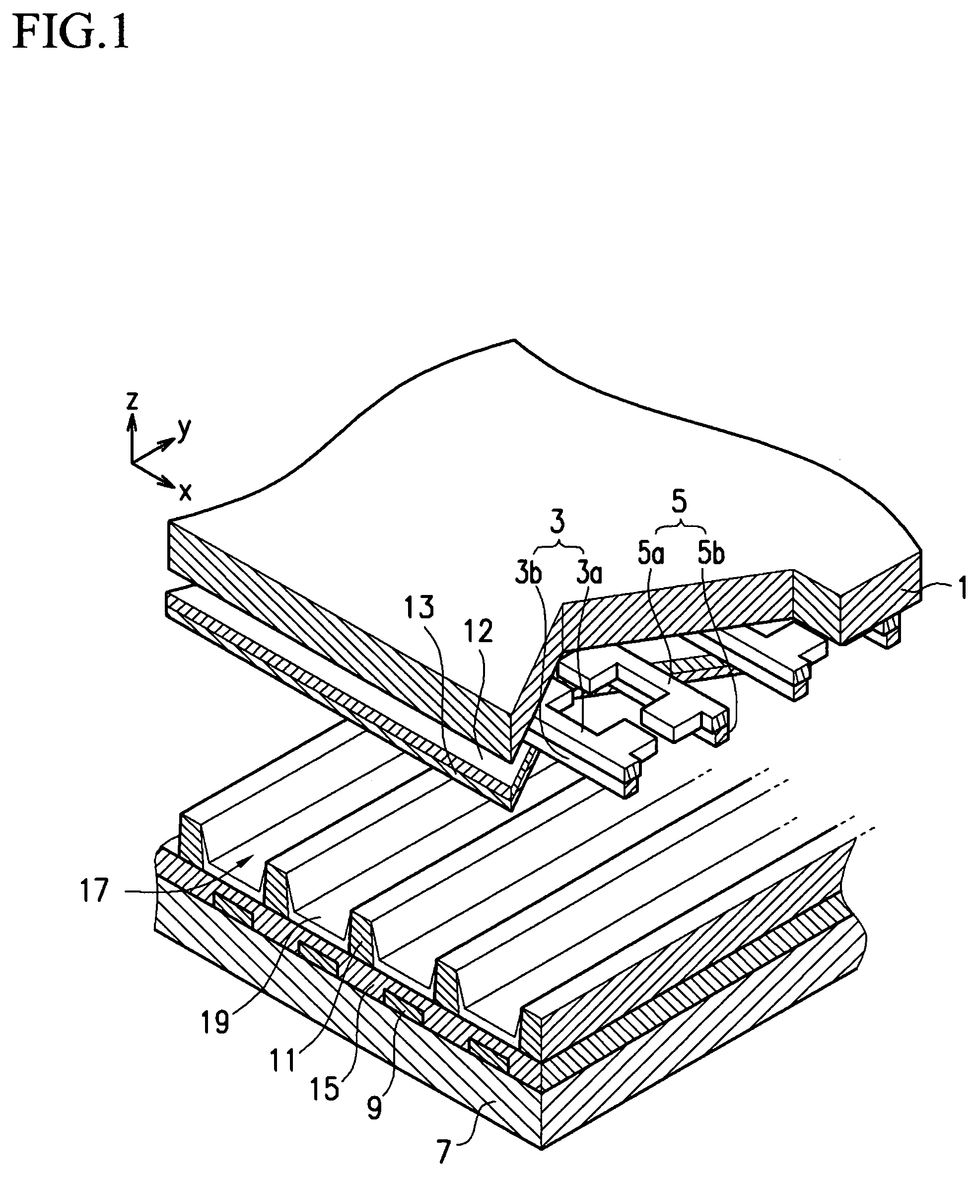
[0034]Turning now to the figures, FIG. 1 is a schematic partial exploded perspective view of a plasma display panel (PDP) according to one embodiment of the present invention. With reference to FIG. 1, the panel includes a first substrate 1 (hereinafter “the front substrate”) having a sustain electrode 3 and a scanning electrode 5 on the inner surface thereof to function as a display electrode, a second substrate 7 (hereinafter “the rear substrate”) having an address electrode 9 on the inner surface thereof, and a barrier rib 11 located between these two substrates 1 and 7. The sustain electrode 3 and the scanning electrode 5 are formed as a pair, and a sustain discharge occurs between the sustain electrode 3 and the scanning electrode 5 when the PDP functions. The sustain electrode 3 and the scanning electrode 5 and the address electrode 9 are formed in a stripe shape on the inner surfaces of the front substrate 1 and the rear substrate 7, respectively. The address electrode 9 cros...


PUM

PropertyMeasurementUnit
transparentaaaaaaaaaa
conductiveaaaaaaaaaa
transparent conductiveaaaaaaaaaa

Abstract

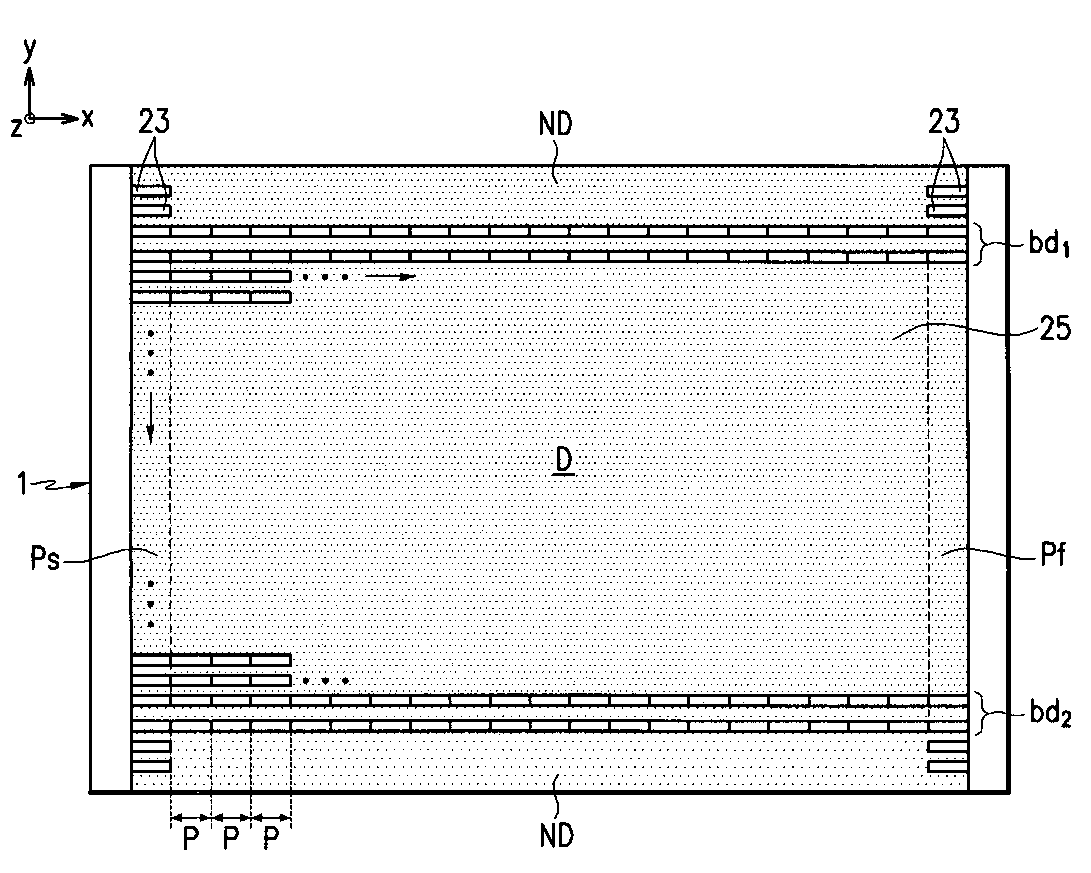
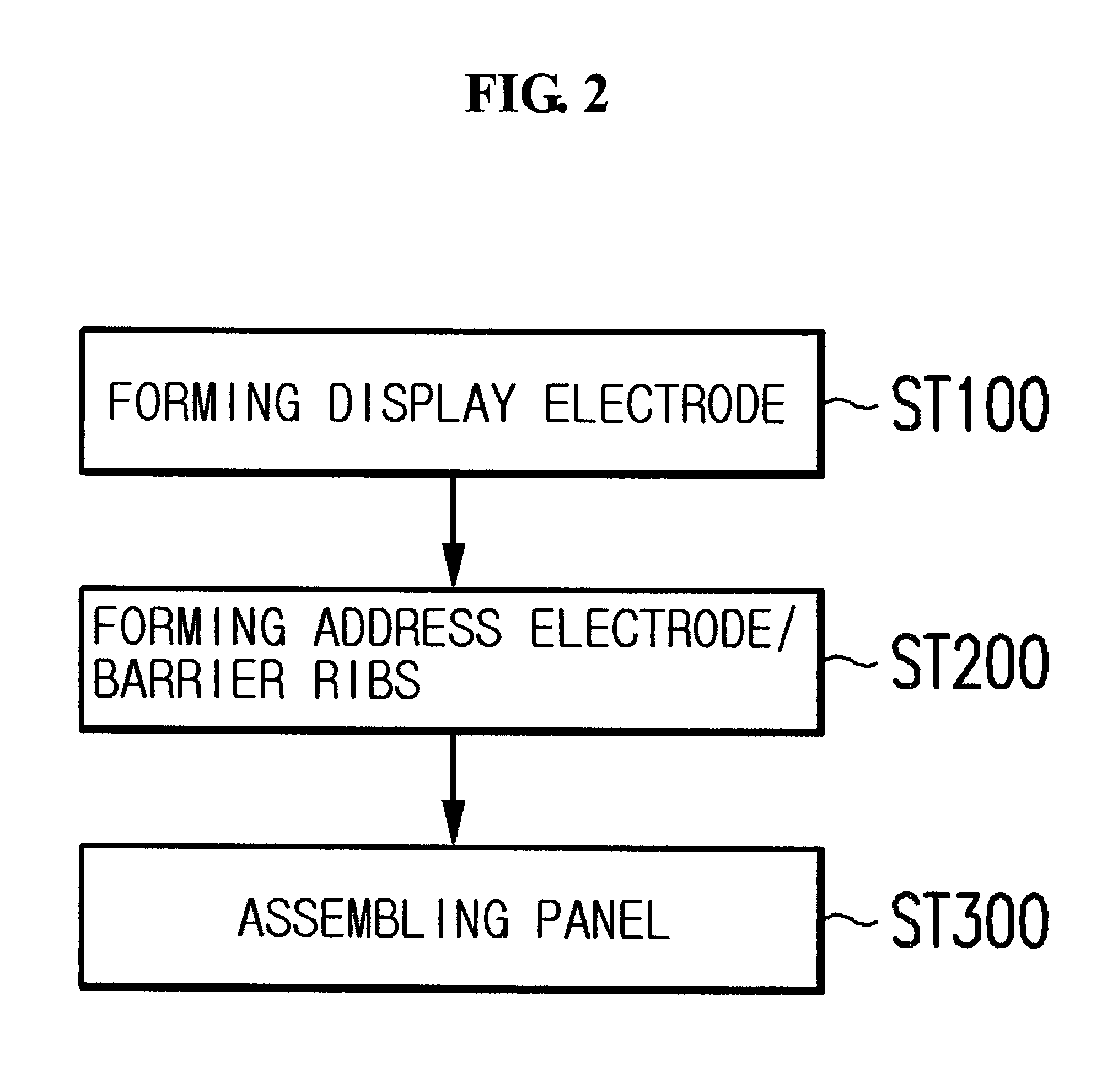
A manufacturing method of a plasma display panel is to form a transparent electrode pattern on a boundary portion between a display region and a non-display region when the transparent electrode pattern is formed by the laser ablation method. The method includes depositing a transparent electrode material layer on a first substrate, patterning the transparent electrode material layer in a display region to form a transparent electrode pattern in the display region, patterning the transparent electrode material layer in a boundary portion to form a transparent electrode pattern in the boundary portion arranged between the display region and a non-display region, depositing a metal conductive layer on the transparent electrode pattern in the display region, patterning the metal conductive layer to form a bus electrode, forming an address electrode and a barrier rib on a second substrate, and aligning and assembling a first plate that includes the first substrate to a second plate that includes the second substrate so that the address electrode and the barrier rib each intersect each of the bus electrode and the transparent electrode pattern in the display region.

Description

CLAIM OF PRIORITY[0001]This application makes reference to, incorporates the same herein, and claims all benefits accruing under 35 U.S.C. §119 from an application earlier filed in the Korean Intellectual Property Office on 10 Dec. 2004 and there duly assigned Ser. No. 10-2004-0104165.BACKGROUND OF THE INVENTION[0002]1. Field of the Invention[0003]The present invention relates to a plasma display panel and a method of manufacturing the same, and more particularly to a plasma display panel where a transparent electrode pattern of a display region is also formed on a boundary portion between the display region and a non-display region, and a method of manufacturing the same.[0004]2. Description of the Related Art[0005]A plasma display panel (PDP) is a display device that displays images using a gas discharge phenomenon. The PDP has superior display characteristics, such as display capacity, brightness, contrast, after-image, and viewing angle.[0006]The PDP generates a gas discharge be...

Claims


Application Information

Patent Timeline
Patent Type & Authority Patents(United States)
IPC IPC(8): H01J17/49H01J9/00H01J9/02H01J11/12H01J11/22H01J11/24H01J11/26H01J11/34
CPCH01J9/02H01J9/185H01J11/12H01J11/22H01J11/34H01J2211/46
Inventor CHOI, JUNG-HYUCKCHIN, YOUNG-HORHO, CHANG-SEOK
Owner SAMSUNG SDI CO LTD
Learn More