Optical device and image display apparatus
an image display and optical device technology, applied in the field of optical devices and image display apparatuses, can solve the problems of reducing the resolution of the display image to be guided to the eye, difficult to achieve different diffraction efficiencies, and difficulty in providing interference fringes, so as to reduce the length of the first diffraction grating member, reduce the thickness of the light guide plate, and increase the range of incident angles
- Summary
- Abstract
- Description
- Claims
- Application Information
AI Technical Summary
Benefits of technology
Problems solved by technology
Method used
Image
Examples
first embodiment
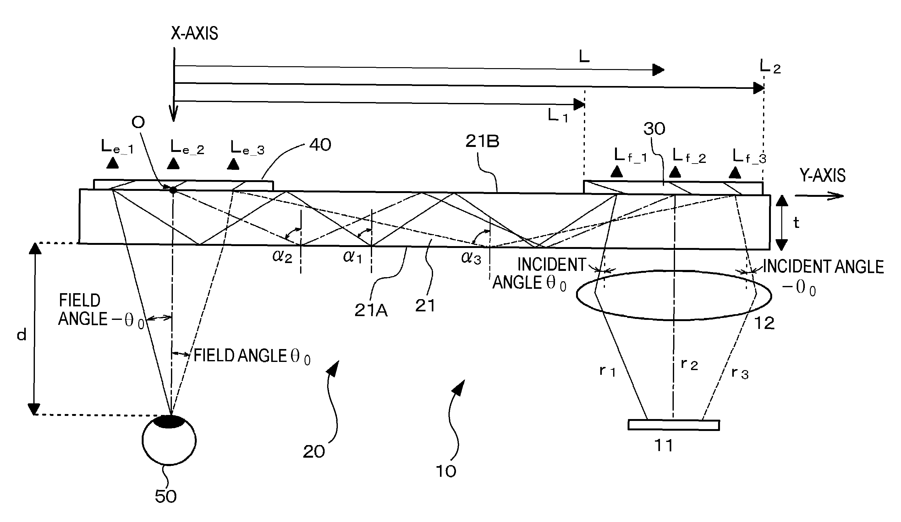
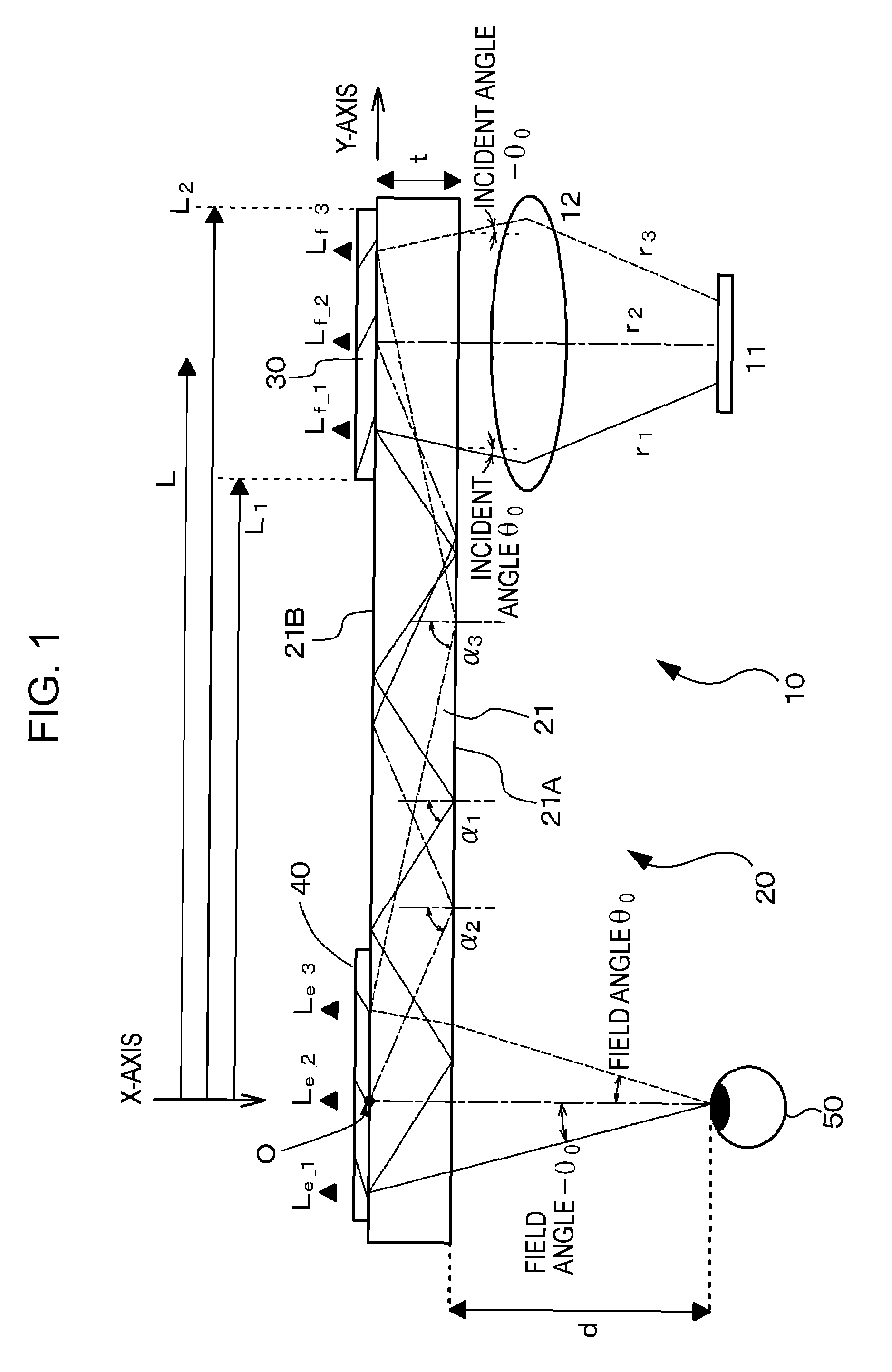
[0084]A first embodiment of the present invention relates to an optical device and an image display apparatus. FIG. 1 schematically illustrates an optical device 20 and an image display apparatus 10 according to the first embodiment of the present invention.
[0085]The image display apparatus 10 according to the first embodiment includes an image forming device 11, a collimator optical unit 12 configured to collimate light beams emitted from the image forming device 11, and the optical device 20 which receives the plurality of collimated beams collimated and oriented in different directions by the collimator optical unit 12, and then guides and emits the collimated beams. The image forming device 11 is, for example, a liquid-crystal display device (LCD). The collimator optical unit 12 is, for example, a convex lens. In order to produce a collimated beam group that includes the plurality of collimated beams traveling in different directions, the image forming device 11 is disposed at a...
second embodiment
[0114]A second embodiment is a modification of the first embodiment. In the second embodiment, the various parameters shown in Table 3 of the first embodiment are changed to parameters shown in Table 6 below.
[0115]
TABLE 6Thickness t of Light Guide Plate 21: 6 mmEye Relief d: 20 mmPitch of Interference Fringes of First Diffraction Grating402.2 nmMember 30:Field Angle θ0: 3.5°Field Angle −θ0: −3.5°
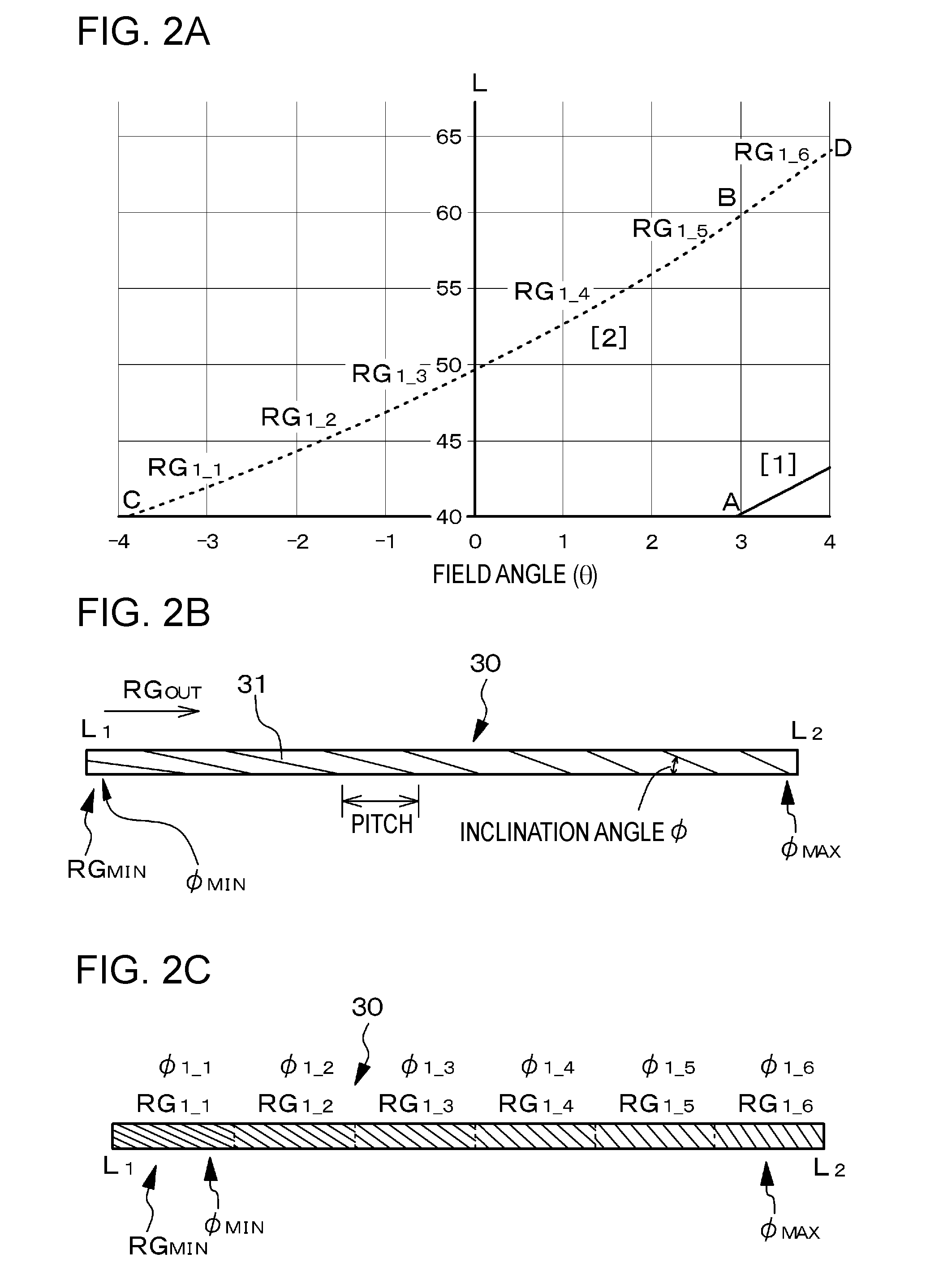
[0116]FIG. 3A is a graph that shows at which point in the first diffraction grating member 30 a collimated beam with a wavelength λ of 522 nm is diffracted and reflected before entering the center of the eye 50, and also shows the number of times the collimated beam undergoes total reflection off the second surface 21B of the light guide plate 21 before reaching the eye 50.
[0117]In FIG. 3A, an upward-sloping solid curve [1] corresponds to a case where the number of times N of total reflection is 3, and an upward-sloping dotted curve [2] corresponds to a case where the number of times N ...
third embodiment
[0127]A third embodiment is also a modification of the first embodiment. In the third embodiment, the various parameters shown in Table 3 of the first embodiment are changed to parameters shown in Table 9 below.
[0128]
TABLE 9Thickness t of Light Guide Plate 21: 5 mmEye Relief d: 20 mmPitch of Interference Fringes of First Diffraction Grating402.2 nmMember 30:Field Angle θ0: 6.0°Field Angle −θ0: −6.0°
[0129]In the third embodiment, the first diffraction grating member 30 includes diffraction grating layers 30A, 30B defined by Q layers of reflective volume hologram diffraction gratings (Q=2 in the third embodiment). Each of the diffraction grating layers 30A, 30B included in the first diffraction grating member 30 has interference fringes extending from within the diffraction grating layer 30A, 30B towards surfaces thereof. The interference fringes on the surfaces of each of the diffraction grating layers 30A, 30B of the first diffraction grating member 30 are arranged at an equal ...
PUM
 Abstract
Description
Claims
Application Information


