Short channel effect engineering in MOS device using epitaxially carbon-doped silicon

a short channel effect and carbon-doped silicon technology, applied in the direction of semiconductor devices, basic electric elements, electrical apparatus, etc., can solve the problems of affecting the performance of transistors, increasing the depth of gate lengths and junctions, and difficulty in implanting impurities only into the desired regions, so as to reduce the diffusion of impurities and reduce the junction depth

Inactive Publication Date: 2009-03-17
TAIWAN SEMICON MFG CO LTD
View PDF9 Cites 3 Cited by
  • Summary
  • Abstract
  • Description
  • Claims
  • Application Information

AI Technical Summary

Benefits of technology

[0008]The advantageous features of the present invention include reduced diffusion of impurities into channel regions of MOS devices and reduced depth of junctions in LDD regions.

Problems solved by technology

In accordance with a design of the metal-oxide-semiconductor (MOS) device and one of the inherent characteristics thereof, modulating the length of a channel region underlying a gate between a source and drain of the transistor alters a resistance associated with the channel region, thereby affecting the performance of the transistor.
When the scales of integrated circuits are reduced to 65 nm and below, further reduction of the gate lengths and junction depths becomes increasingly difficult.
In addition, the implantation process has the drawback of having boundaries with a slowly changing impurity concentration, and thus it is difficult to implant impurities only into the desired regions.

Method used


Image

  • Short channel effect engineering in MOS device using epitaxially carbon-doped silicon
  • Short channel effect engineering in MOS device using epitaxially carbon-doped silicon
  • Short channel effect engineering in MOS device using epitaxially carbon-doped silicon

Examples


Embodiment Construction

[0014]The making and using of the presently preferred embodiments are discussed in detail below. It should be appreciated, however, that the present invention provides many applicable inventive concepts that can be embodied in a wide variety of specific contexts. The specific embodiments discussed are merely illustrative of specific ways to make and use the invention, and do not limit the scope of the invention.

[0015]A novel method for forming a metal-oxide semiconductor (MOS) device is provided. The intermediate stages of manufacturing a preferred embodiment of the present invention are illustrated in FIGS. 1 through 8A. Variations of the preferred embodiments are then discussed. Throughout the various views and illustrative embodiments of the present invention, like reference numbers are used to designate like elements.

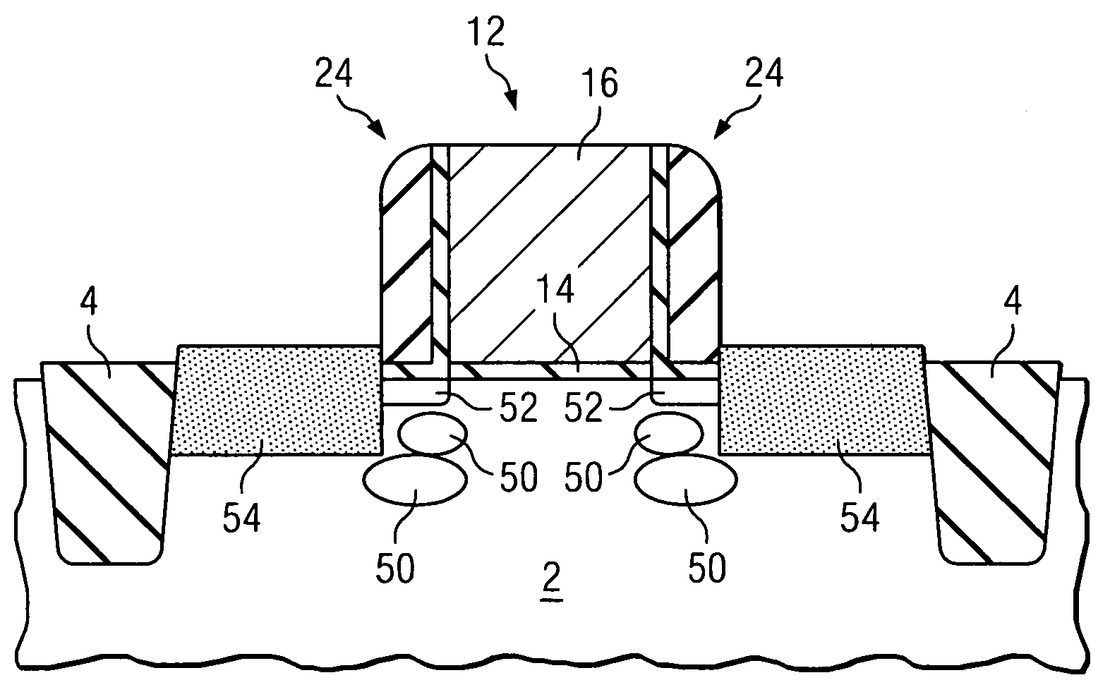
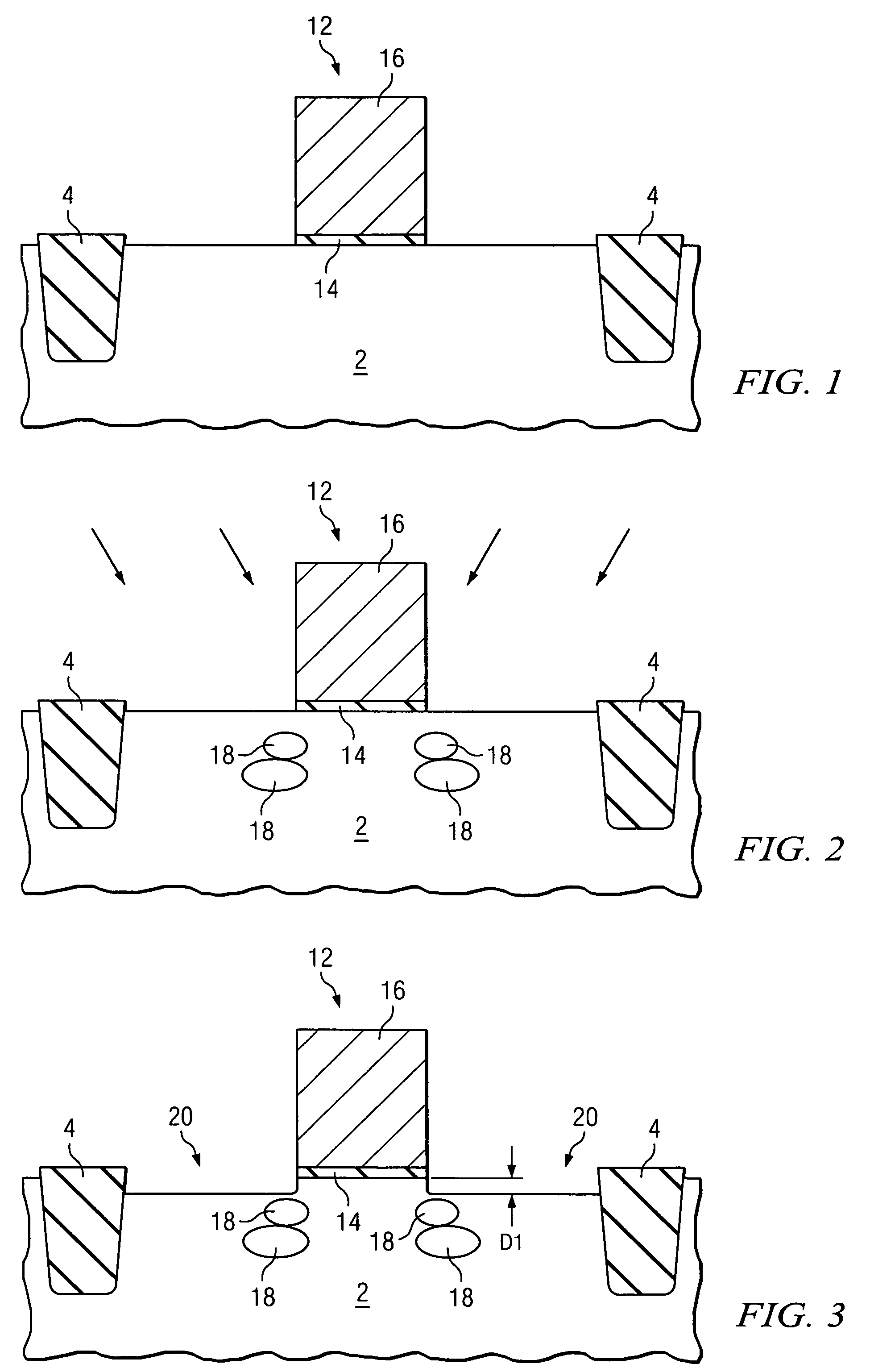
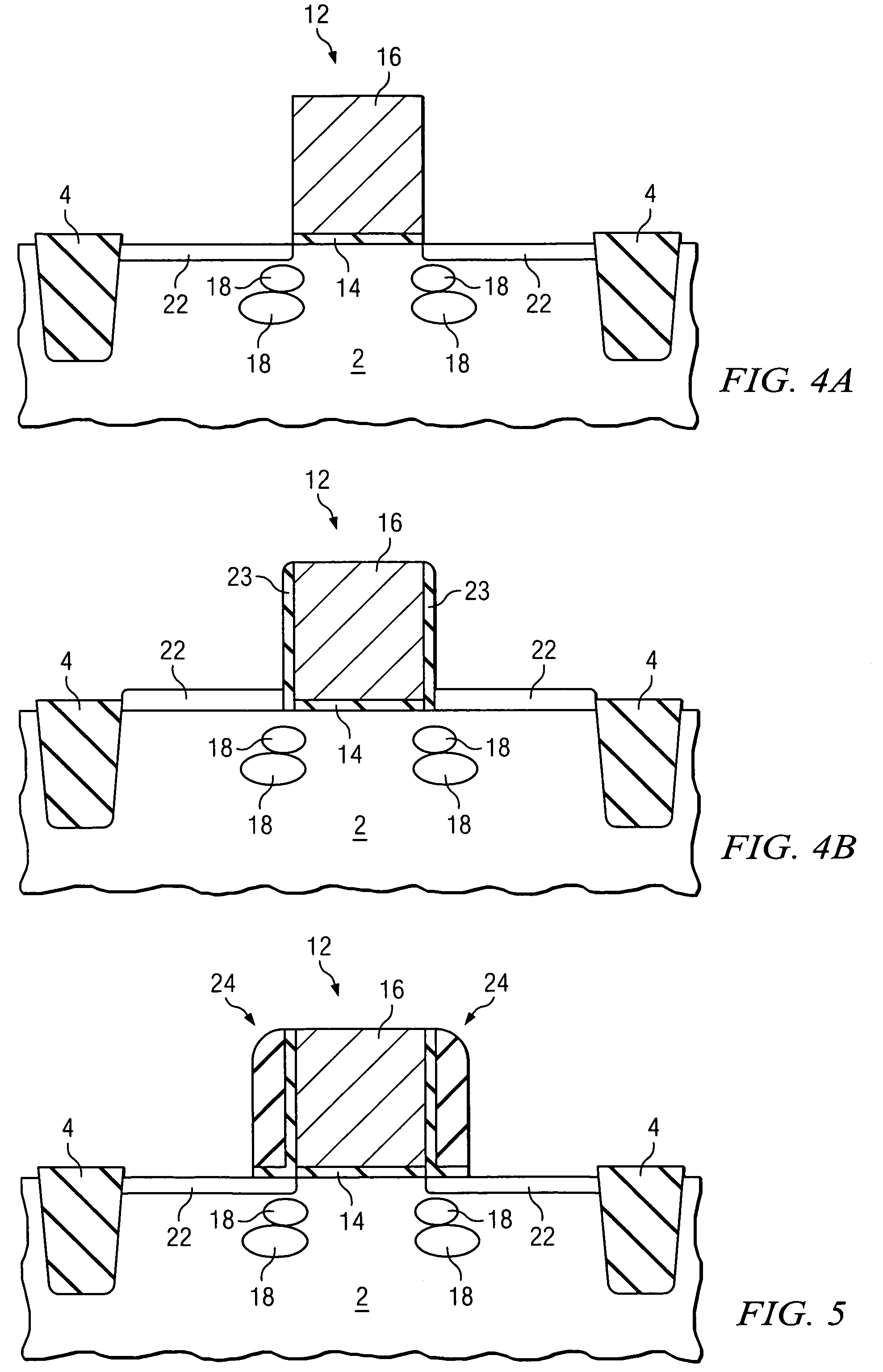
[0016]FIG. 1 illustrates a gate stack 12 formed on a substrate 2. Preferably, substrate 2 comprises bulk silicon. Alternatively, substrate 2 comprises bulk SiGe or ...


PUM


Abstract

A method for forming a semiconductor structure includes providing a semiconductor substrate, forming a gate stack on the semiconductor substrate, and epitaxially growing a lightly-doped source / drain (LDD) region adjacent the gate stack, wherein carbon is simultaneously doped into the LDD region.

Description

TECHNICAL FIELD[0001]This invention relates generally to integrated circuits, and more particularly to structure and formation methods of MOS devices.BACKGROUND[0002]Reductions in the size and inherent features of semiconductor devices (e.g., a metal-oxide semiconductor field-effect transistor) have enabled continued improvements in speed, performance, density, and cost per unit function of integrated circuits over the past few decades. In accordance with a design of the metal-oxide-semiconductor (MOS) device and one of the inherent characteristics thereof, modulating the length of a channel region underlying a gate between a source and drain of the transistor alters a resistance associated with the channel region, thereby affecting the performance of the transistor. More specifically, shortening the length of the channel region reduces a source-to-drain resistance of the transistor, which assuming other parameters are maintained relatively constant, may allow an increase in current...

Claims


Application Information

Patent Timeline
Patent Type & Authority Patents(United States)
IPC IPC(8): H01L21/00H01L21/336H01L21/84
CPCH01L21/26513H01L21/26586H01L29/1083H01L29/6656H01L29/66628H01L29/66636H01L29/7833H01L29/7848H01L29/665H01L21/2658
Inventor KU, KEH-CHIANGTSAI, PANG-YENNIEH, CHUN-FENGWANG, LI-TING
Owner TAIWAN SEMICON MFG CO LTD
Why Eureka
Try Eureka