Method of manufacturing ceramic paste and ceramic multi-layer wiring substrate utilizing the same

a multi-layer wiring and ceramic technology, applied in the direction of electrical equipment, conductive materials, solid-state devices, etc., can solve the problems of layer bonding failure or so-called delamination and warping deformation, internal wiring gap generation during formation of internal wiring, etc., to prevent internal wiring deformation, layer bonding, and sufficient fluidity

Inactive Publication Date: 2009-03-24
KYOCERA CORP
View PDF10 Cites 12 Cited by
  • Summary
  • Abstract
  • Description
  • Claims
  • Application Information

AI Technical Summary

Benefits of technology

[0017]The invention has been completed taking the problems into consideration, and it is an object of the invention to provide a method of manufacturing a ceramic paste and a ceramic multi-layer wiring substrate utilizing the same, in which a region having no internal wiring formed therein is filled with a ceramic paste which is highly suitable for screen printing and which is properly balanced with an internal wiring in viscoelasticity; a subsequent pressure leveling step is performed under a heating condition that is equal to or higher than the glass-transition temperature of an acryl type binder in the ceramic paste to provide the ceramic paste with sufficient fluidity without increasing the amount of a plasticizer or solvent and to thereby prevent deformation of the internal wiring; and thus, a layer bonding failure and warping deformation of the ceramic multi-layer wiring substrate can be more effectively prevented.

Problems solved by technology

Particularly, under the circumstance in which ceramic multi-layer wiring substrates are becoming thinner, gaps in such a substrate generated during formation of an internal wiring due to a height difference attributable to the thickness of the internal wiring are difficult to eliminate completely during layer stacking by utilizing only plastic deformation of a green sheet whose thickness is small.
As a result, there arises a problem that a layer bonding failure or so-called delamination and warping deformation can occur in such a product after it is fired.
However, a green sheet having a ceramic filling layer obtained by the screen printing process has a problem in that the layer pattern can bulge at edges thereof due to surface tension when the screen is separated from the same, and a phenomenon also occurs in which the pattern bulges in a substantially semicircular or semi-elliptic shape when the pattern is constituted by very fine lines having a great thickness.
It is therefore difficult to eliminate irregularities on the surface of the sheet completely, and it is required to add a step for pressing the sheet with a surface-leveling press to level the same.
However, since a ceramic paste utilizing a cellulose type binder has low fluidity, it is difficult to level the paste sufficiently at the pressure leveling step.
However, when the balance of viscoelastic properties of ceramic pastes is not properly controlled, it is difficult to level a ceramic paste without deforming an internal wiring pattern adjacent to the ceramic paste if the pressure leveling is performed under a temperature condition that is equal to or higher than the glass-transition temperature of an acryl type binder added to the ceramic paste.
As a result, there is a high possibility of the problem that the internal wiring is significantly deformed.
When an acryl type binder is used without adjusting its molecular weight properly, a problem is frequently created by spinnability that is a shortcoming of the use of an acryl type binder in screen printing.
When a plasticizer and solvent are excessively used, a ceramic paste tends to have high viscosity attributable to insufficient drying even if a drying step is performed after screen printing.
Therefore, a resultant printed material may remain viscous or may have low strength, which results in a problem in that the printed material can be subjected to cohesive breakage or interfacial breakage and transferred to a surface of the press during the pressure leveling step.

Method used


Image

  • Method of manufacturing ceramic paste and ceramic multi-layer wiring substrate utilizing the same
  • Method of manufacturing ceramic paste and ceramic multi-layer wiring substrate utilizing the same

Examples


example

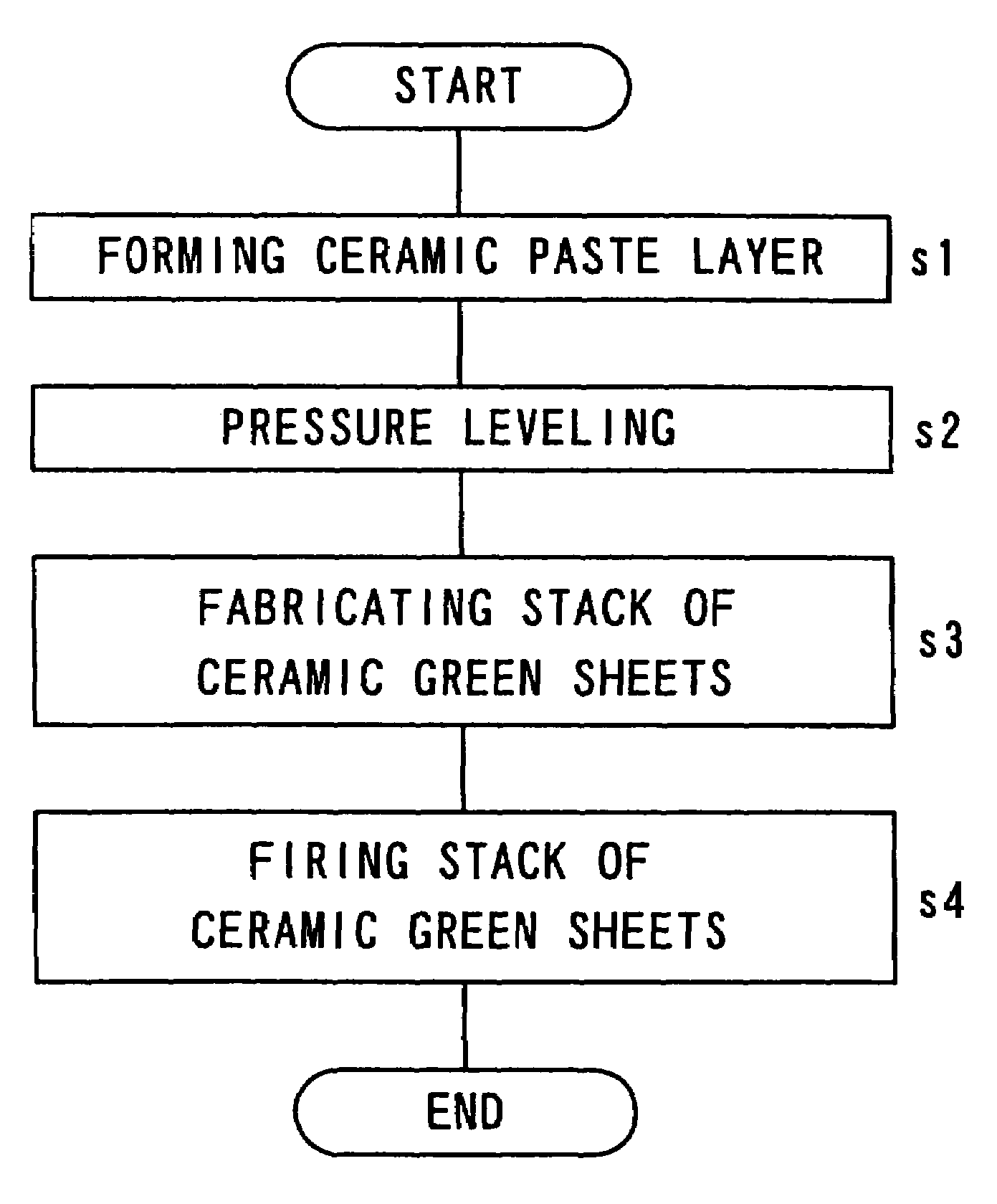
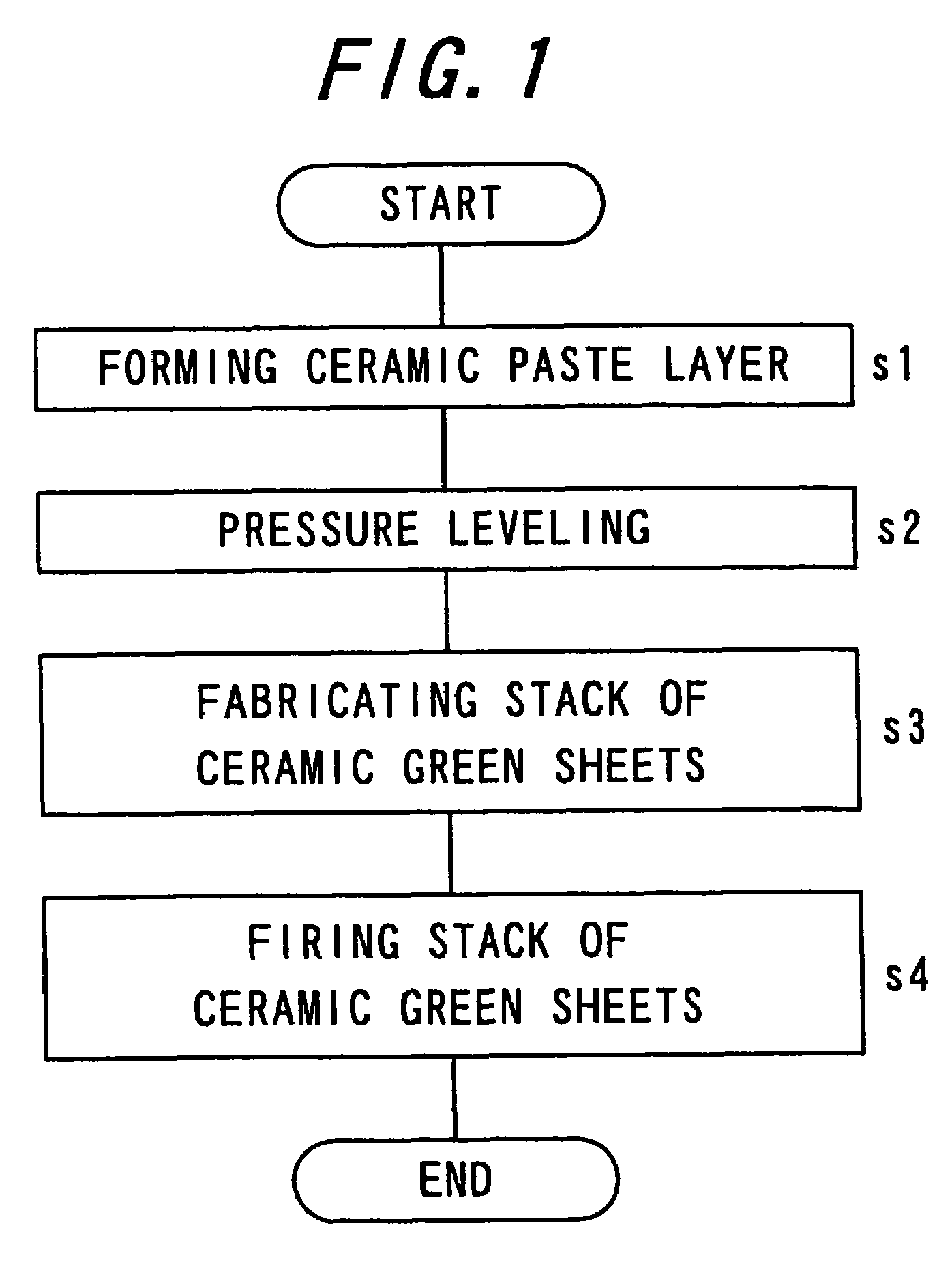
[0079]Examples of the method of manufacturing a ceramic paste and a ceramic multi-layer wiring substrate according to the invention will now be described.

[0080][Measurement of Loss Factor tan δ]

[0081]A rheology measuring apparatus (Model MCR300 manufactured by Physica Messtechnik BmbH) was used for measurement of loss factor tan δ represented by (loss modulus) / (storage modulus) described in the present embodiment. A ceramic paste and a conductor paste to be an internal wiring were printed using a screen printing machine such that the ceramic paste and the conductor paste wound be in the form of sheets each having a thickness of 100 μm, and the ceramic paste and the conductor paste were dried for one hour at 80° C. using a hot-air drying oven. The dried sheet-like materials were set in a metal mold of a pressing machine and were pressed at a pressure of 4.9×10⁶ Pa to fabricate samples for measurement in the form of disks having a thickness of 0.5 mm and a diameter of 20 mm.

[0082]A di...

examples 1 to 10

[0083]A binder, additives such as a plasticizer, and an organic solvent were added to a mixed powder of alumina type ceramics mainly composed of alumina to prepare slurry, and the slurry was molded using a doctor blade process and then dried to fabricate a green sheet of 50 mm horizontal×50 mm vertical×0.3 mm thick size.

[0084]Next, to 100 parts by weight of mixed powders of alumina type ceramics mainly composed by alumina, 5 parts by weight of a binder having percentages of composition as shown in Table 1 below, 20 parts by weight of a mixed solvent of terpineol and butyl carbitol acetate, and 20 parts by weight of a phthalate ester type plasticizer (a mixture of DOP and DBP) were added and agitated to be mixed. Thereafter, mixing was performed using a triple roll mill until aggregates of the ceramic powders and the binder were eliminated to prepare ceramic pastes.

[0085]To 100 parts by weight of a tungsten powder, 1.5 parts by weight of a binder composed of an acrylic resin and nitr...


PUM

PropertyMeasurementUnit
glass-transition temperatureaaaaaaaaaa
temperatureaaaaaaaaaa

Abstract

In manufacturing a ceramic multi-layer wiring substrate which is formed by stacking a plurality of ceramic layers and which includes an internal wiring, a ceramic paste is printed using a screen printing process on a part of a ceramic green sheet to be a ceramic layer having the internal wiring formed thereon which part does not include the internal wiring, to form between the ceramic layers a ceramic filling layer including a same ceramic component as that in the ceramic layers which ceramic filling layer is not formed on the internal wiring. The ceramic paste includes a ceramic component, an acrylic resin, and a cellulose resin, and loss factor tan δ of the paste represented by (loss modulus) / (storage modulus) in a dry condition after printing is equal to or greater than loss factor tan δ of a conductor paste layer to be the internal wiring in a dry condition.

Description

BACKGROUND OF THE INVENTION[0001]1. Field of the Invention[0002]The present invention relates to a method of manufacturing a ceramic paste and a ceramic multi-layer wiring substrate having an internal wiring utilizing the same. More particularly, the invention relates to a method of manufacturing a ceramic multi-layer wiring substrate formed by a plurality of ceramic layers stacked one on top of another and having an internal wiring, in which a ceramic filling layer including the same ceramic component as that in the ceramic layers is formed in a region having no internal wiring formed therein between the ceramic layers stacked so that the internal wiring is sandwiched therebetween. More specifically, the invention relates to a method of manufacturing a ceramic paste which is preferable for fabricating a ceramic green sheet having substantially no irregularity and thereby preventing a layer bonding failure and warping deformation of a ceramic multi-layer wiring substrate more effect...

Claims


Application Information

Patent Timeline
Patent Type & Authority Patents(United States)
IPC IPC(8): C03C8/16H01B1/02B32B3/00H01L23/498H05K1/03H05K3/46
CPCB32B18/00C04B35/63C04B35/632C04B35/634H01L23/49883H05K3/4629Y10T428/24926B32B2311/06B32B2311/08B32B2311/09B32B2311/12C04B2235/3206C04B2235/3217C04B2235/3222C04B2235/3231C04B2235/3244C04B2235/3418C04B2235/3463C04B2235/3481C04B2235/365C04B2235/48C04B2235/6025C04B2235/604C04B2235/96C04B2237/403C04B2237/407C04B2237/408C04B2237/62C04B2237/704H01L2924/09701H05K1/0306H05K2201/09881H01L2924/0002B32B2311/04H01L2924/00
Inventor TAKASE, HIROYUKISUZUKI, SHINICHIIKI, YUTAKA
Owner KYOCERA CORP
Why Eureka
Try Eureka