Method of fabricating multi-fin field effect transistor

a field effect transistor and multi-fin technology, applied in the field of field effect transistors, can solve the problems of floating body effect, affecting reliability and stability of the semiconductor device, and the problem of not solving the problems of the conventional semiconductor device with a vertical gate structure,

Active Publication Date: 2009-03-31
PROMOS TECH INC
View PDF2 Cites 2 Cited by
  • Summary
  • Abstract
  • Description
  • Claims
  • Application Information

AI Technical Summary

Benefits of technology

[0009]Accordingly, one objective of the present invention is to provide a multi-fin field effect transistor, so as to avoid the floating body effect and the problems caused by the epitaxial process.
[0010]Another objective of the present invention is to provide a method of fabricating a multi-fin field effect transistor, so as to inhibit the float body effect and enhance reliability and stability of a device.
[0013]The multi-fin field effect transistor and the fabricating method thereof provided by the present invention have a multi-channel structure, thus the electrical capacity of a device is increased, so as to improve the efficiency of the device and avoid the floating body effect caused by excessive accumulation of charges. In addition, the present invention does not employ the epitaxial process and thus does not have the problems such as the process takes a long time, the surface of the epitaxial layer is always difficult to be cleaned, and the process cannot be readily controlled and generates facet effect, thereby influencing subsequent processes.

Problems solved by technology

However, the conventional semiconductor device with a vertical gate structure still has some problems that are not solved.
For example, the most serious problem of the conventional device is the floating body effect.
Furthermore, the floating body effect causes the semiconductor device turn on automatically without applying a voltage, thereby influencing reliability and stability of the semiconductor device and causing leakage current.
However, the epitaxial process takes a long time and it is always difficult to clean the surface of an epitaxial layer.
In addition, the epitaxial process cannot be readily controlled, resulting in facet effect and influencing the subsequent processes.

Method used


Image

  • Method of fabricating multi-fin field effect transistor
  • Method of fabricating multi-fin field effect transistor
  • Method of fabricating multi-fin field effect transistor

Examples


Embodiment Construction

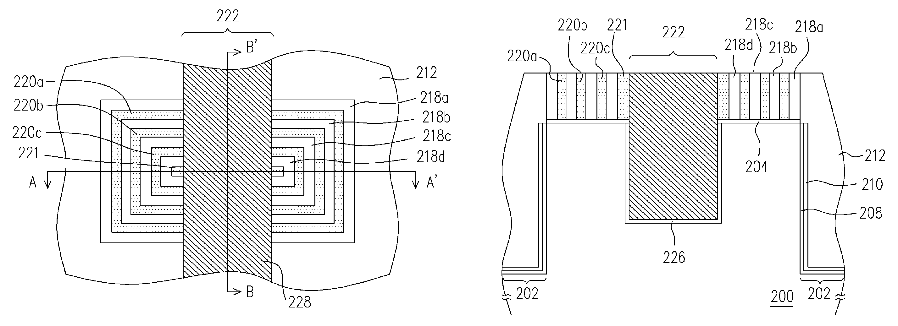
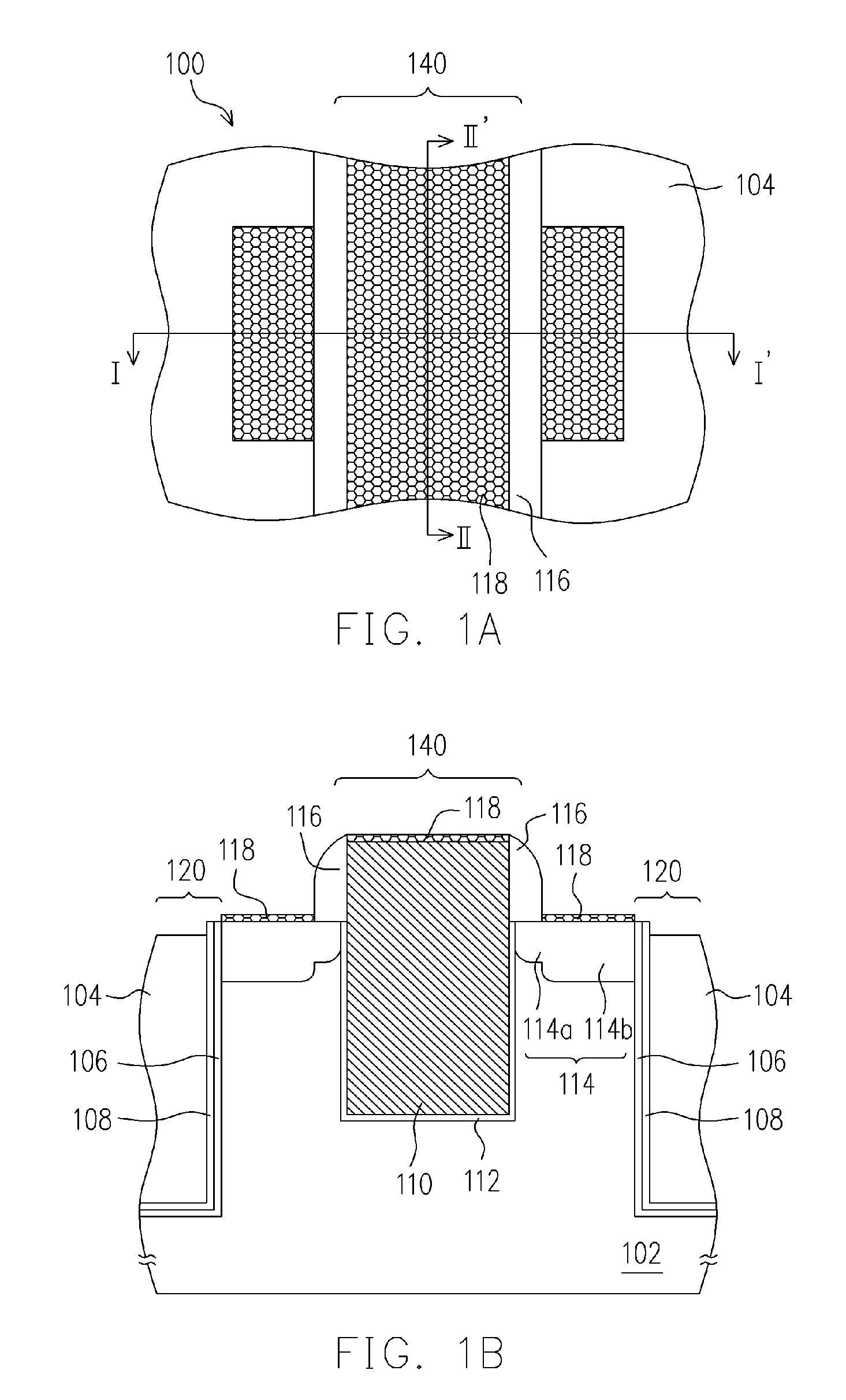
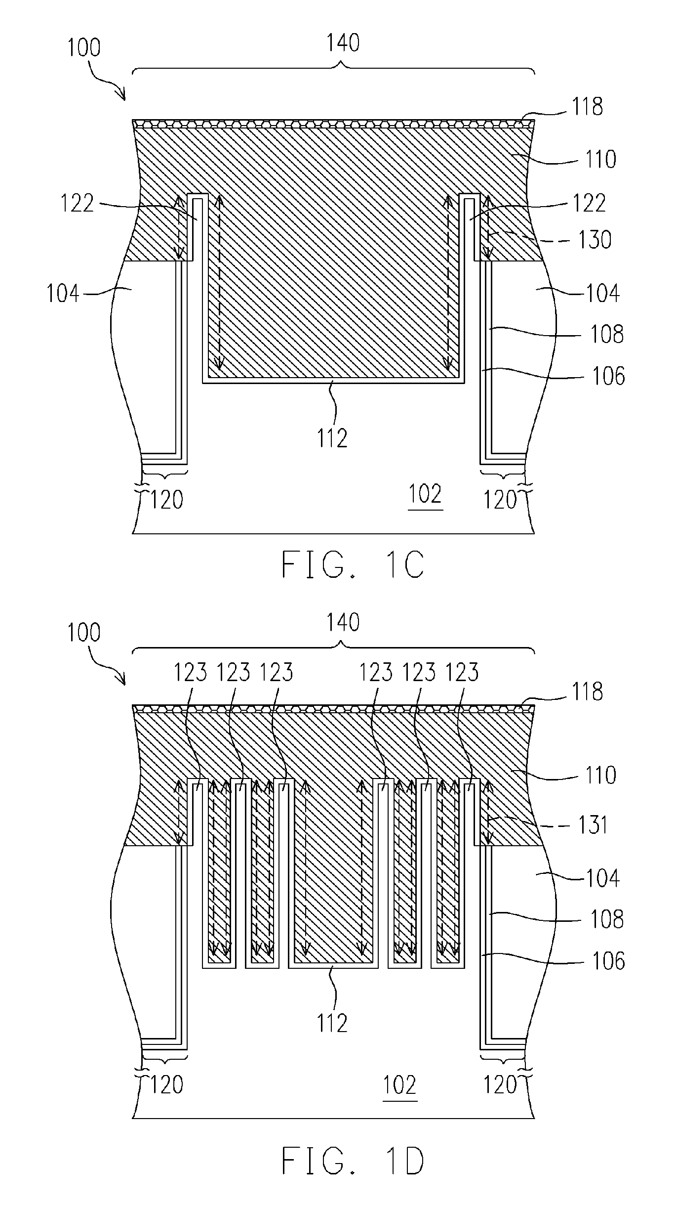
[0023]FIG. 1A is a top view of the multi-fin field effect transistor according to one embodiment of the present invention. FIG. 1B is a schematic sectional view of FIG. 1A along the section line I-I′. FIG. 1C is a schematic sectional view of FIG. 1A along the section line II-II′. FIG. 1D is a schematic sectional view of FIG. 1A along the section line II-II′ according to another embodiment of the present invention.

[0024]Referring to FIGS. 1A, 1B and 1C, the multi-fin field effect transistor 100 in the embodiment comprises a substrate 102, an oxide layer 104, a conductive layer 110, a gate oxide layer 112, and a doped region 114. The substrate 102 is, for example, a silicon substrate. The region 102 surrounded by a trench 120 is an active region of a transistor, and at least two fin-type silicon layers 122 are formed in the substrate 102 in a region 140 prepared to form a gate. The oxide layer 104 is disposed in the trench 120, and the top surface of the oxide layer 104 is lower than ...


PUM


Abstract

A multi-fin field effect transistor includes a substrate, an oxide layer, a conductive layer, a gate oxide layer, and a doped region is provided. The substrate is surrounded by a trench, and there are at least two fin-type silicon layers formed in the substrate in a region prepared to form a gate thereon. The oxide layer is disposed in the trench and the top surface of the oxide layer is lower than that of the fin-type silicon layers. The conductive layer is disposed in the region prepared to form a gate. The top surface of the conductive layer is higher than that of the fin-type silicon layers. The gate oxide layer is disposed between the conductive layer and the fin-type silicon layers and disposed between the conductive layer and the substrate. The doped region is disposed in the substrate on both sides of the conductive layer.

Description

CROSS-REFERENCE TO RELATED APPLICATION[0001]This application claims the priority benefit of Taiwan application serial no. 95119811, filed on Jun. 5, 2006. All disclosure of the Taiwan application is incorporated herein by reference.BACKGROUND OF THE INVENTION[0002]1. Field of Invention[0003]The present invention relates to a field effect transistor and a fabricating method thereof, and more particularly to a multi-fin field effect transistor and a fabricating method thereof.[0004]2. Description of Related Art[0005]With the device size gradually shrunken, in order to satisfy multiple applications of an integrated circuit in future, currently, the transistor shape of a semiconductor device is developed from a planar gate structure to a vertical gate structure.[0006]Now, some patents have disclosed relevant technology focusing on this aspect. For example, US Patent No. 2004 / 0227181 has disclosed a multi-channel transistor and a fabricating method thereof. The aforementioned document is...

Claims


Application Information

Patent Timeline
Patent Type & Authority Patents(United States)
IPC IPC(8): H01L21/336
CPCH01L29/66795H01L29/7851
Inventor WU, HSIAO-CHE
Owner PROMOS TECH INC
Why Eureka
Try Eureka