Bulk resistance control technique

a control technique and resistance technology, applied in the direction of resistors, basic electric elements, solid-state devices, etc., can solve the problems of increased self-heating, high cost of starting materials, floating body and history effects,

Active Publication Date: 2009-03-31
SOFICS BVBA
View PDF11 Cites 15 Cited by
  • Summary
  • Abstract
  • Description
  • Claims
  • Application Information

AI Technical Summary

Problems solved by technology

However, SOI technology comes also with a few disadvantages such as the higher cost for starting material, floating body and history effects, increased self-heating issues and higher design complexity.
Another main disadvantage is the fact that traditional snap-based ESD solutions have a much reduced (It2) failure current.
Since the avalanche multiplication causes heat, reducing the avalanche multiplication can increase the failure current It2 of the MOS device.
The disadvantage with this technique is that the bulk connection is only at the both sides of the gate.
However, in some technologies the STI does not reach to the box either.
The disadvantage of this technique is similar to the technique discussed in FIG. 1 that the bulk connection is only at the both sides of the gate.
Another disadvantage is that an extra process option, for example PTI is needed.
Since extra process steps are very costly, this technique is undesirable.
The disadvantage if this technique is that the bulk connection is always shorten to the source.

Method used


Image

  • Bulk resistance control technique
  • Bulk resistance control technique
  • Bulk resistance control technique

Examples


Embodiment Construction

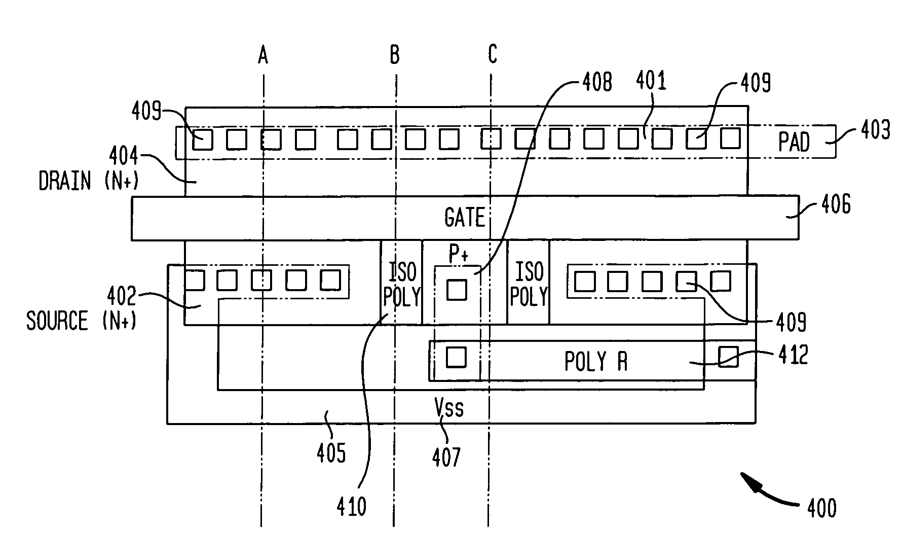
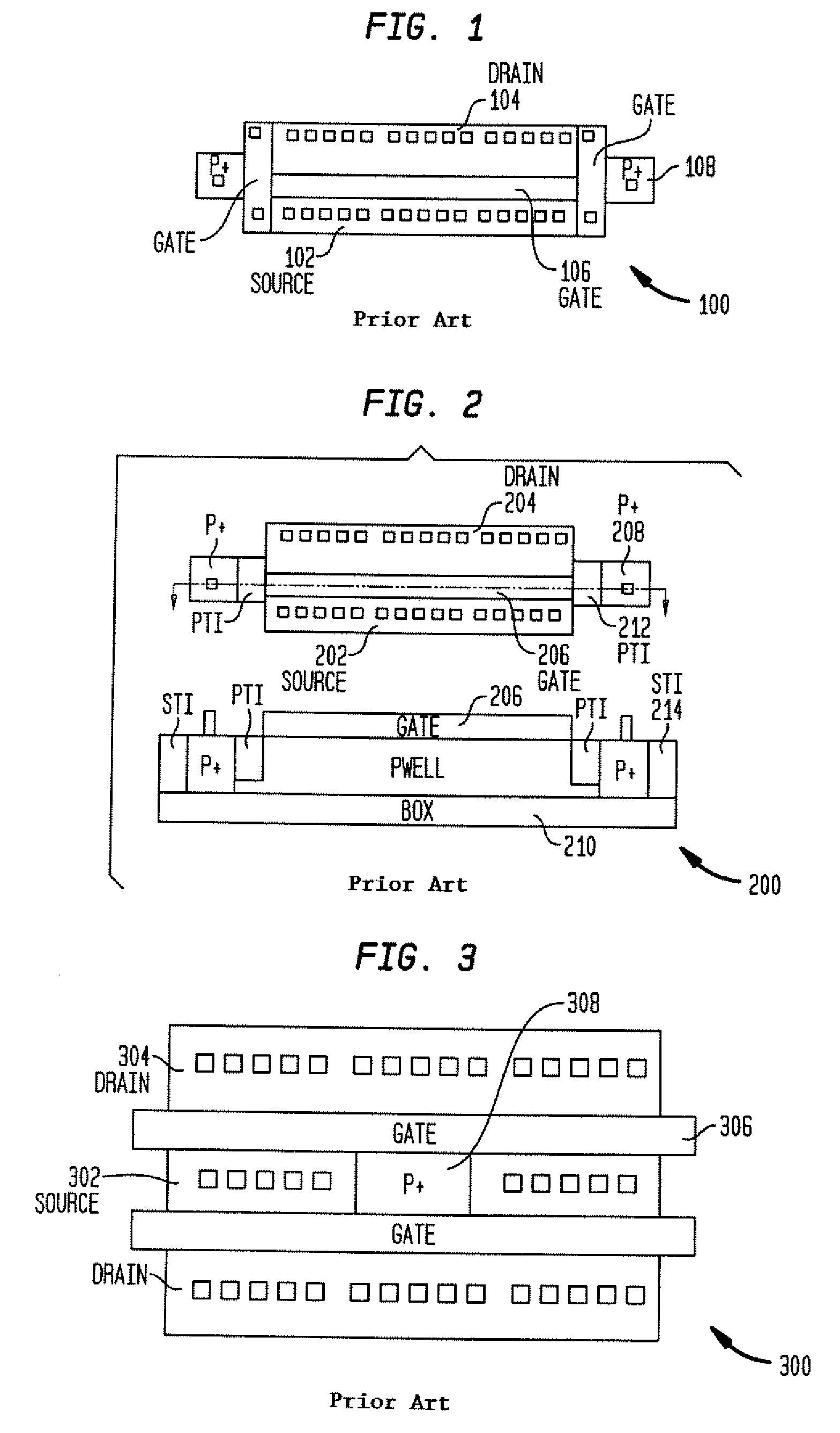
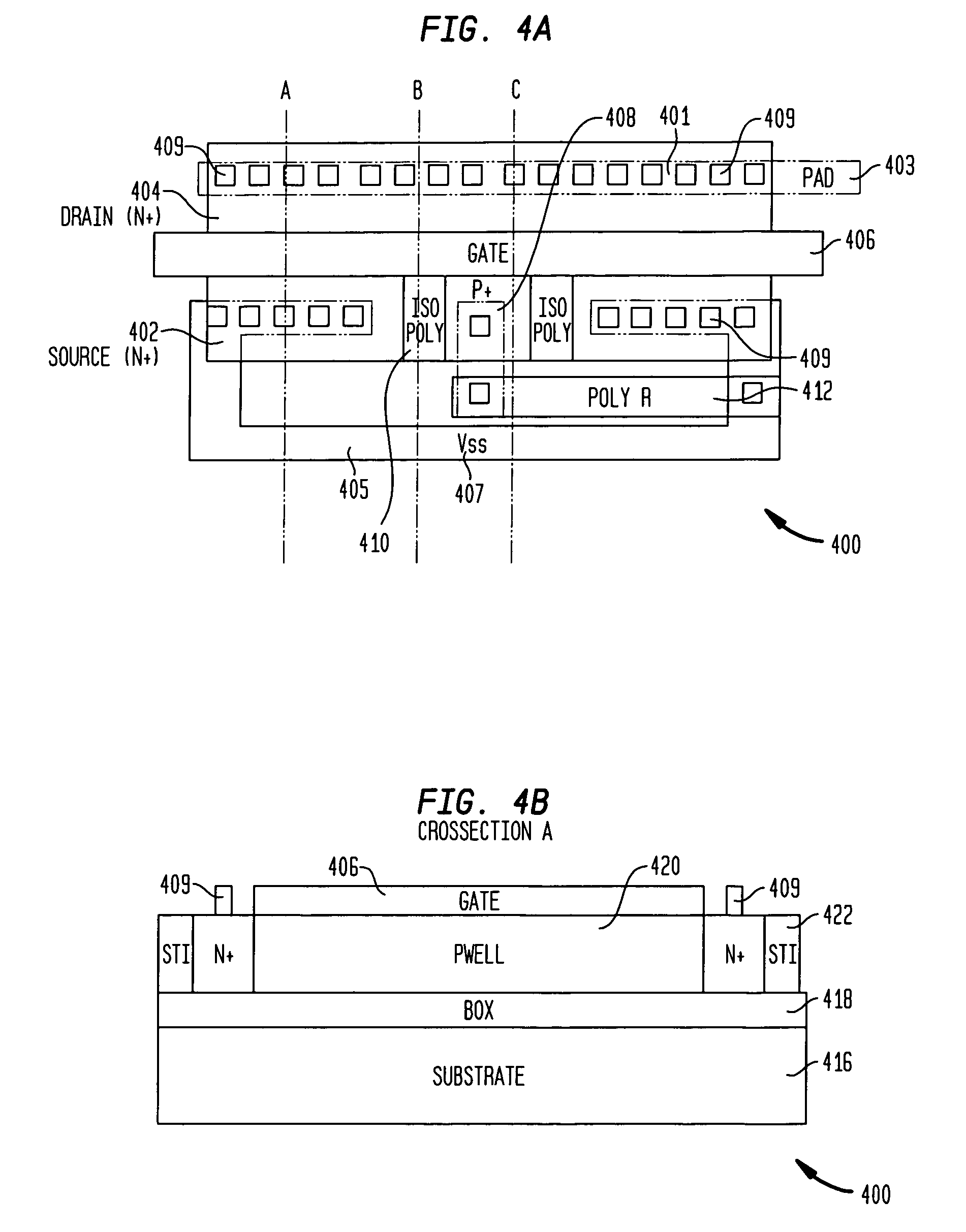
[0026]The process steps and structures described below do not form a complete process flow for manufacturing integrated circuits (ICs). The present invention can be practiced in conjunction with silicon-on-insulator (SOI) integrated circuit fabrication techniques currently used in the art, and only so much of the commonly practiced process steps are included as are necessary for an understanding of the present invention. The figures representing cross-sections and layouts of portions of an IC during fabrication are not drawn to scale and form, but instead are drawn so as to illustrate the important features of the invention.

[0027]The present invention is described with reference to SOI CMOS devices. However, those of ordinary skill in the art will appreciate that selecting different dopant types and adjusting concentrations or changing the isolation types allows the invention to be applied to other processes that are susceptible to damage caused by ESD. Furthermore, it is noted that...


PUM


Abstract

The present invention provides a MOS transistor device for providing ESD protection including at least one interleaved finger having a source, drain and gate region formed over a channel region disposed between the source and the drain regions. The transistor device further includes at least one isolation gate formed in at least one of the interleaved fingers. The device can further include a bulk connection coupled to at least one of the source, drain and gate regions via through at least one of diode, MOS, resistor, capacitor inductor, short, etc. The bulk connection is preferably isolated through the isolation gate.

Description

CROSS REFERENCES[0001]This patent application claims the benefit of U.S. Provisional Application Ser. No. 60 / 692,675 filed Jun. 21, 2005, the contents of which are incorporated by reference herein.FIELD OF THE INVENTION[0002]This invention generally relates to the field of electrostatic discharge (ESD) protection circuitry, and more specifically, for providing a technique for implementing bulk connection to improve the performance of metal oxide semiconductor (MOS) devices in the silicon over insulator (SOI) protection circuitry of an integrated circuit (IC).BACKGROUND OF THE INVENTION[0003]Recently, advanced SOI technology nodes are being used more extensively due to a number of advantages mainly related to the reduction of the power consumption, smaller silicion area, lower gate delay and reduced parasitic junction capacitance. Moreover, due to the completely isolated transistors, latch-up is no longer an issue.[0004]However, SOI technology comes also with a few disadvantages such...

Claims


Application Information

Patent Timeline
Patent Type & Authority Patents(United States)
IPC IPC(8): H01L23/62H01L27/10H01L29/72H01L29/73H01L29/74H01L29/76H01L29/94H01L31/062H01L31/111H01L31/113H01L31/119
CPCH01L27/0277
Inventor VAN CAMP, BENJAMINVERMONT, GERD
Owner SOFICS BVBA
Why Eureka
Try Eureka