Electrical Antifuse and Method of Programming

a technology of anti-fuses and circuits, applied in the direction of electrical equipment, semiconductor devices, semiconductor/solid-state device details, etc., can solve the problems of high programming voltage, severe trade-offs, and numerous serious drawbacks of anti-fuses, and achieve rapid and reliable programming, low voltage, and simple design

Active Publication Date: 2009-12-31
MARVELL ASIA PTE LTD
View PDF46 Cites 6 Cited by
  • Summary
  • Abstract
  • Description
  • Claims
  • Application Information

AI Technical Summary

Benefits of technology

[0008]It is therefore an object of the present invention to provide an antifuse structure of simple design which can be fabricated at a small size using processes which are compatible with formation of other devices using other technologies, particularly CMOS technology, and which can be rapidly and reliably programmed with a relatively low voltage and current with low heat generation.
[0013]According to the present invention, a method of programming an antifuse having an anode, a cathode, and a link containing an unsilicided portion is provided. The method comprises the steps of electromigrating a silicide containing material into the unsilicided portion of the link; and reducing the resistance of the antifuse.
[0015]According to the present invention, the method may include a further step of electromigrating material from the link toward the anode to form an electromigrated semiconductor portion in the link which does not contain a significant concentration of silicide or a silicide alloy but substantially contains only a semiconductor material. Alternatively, the material may be electromigrated from the link toward the cathode to form an electromigrated semiconductor portion in the link. The resistance of the antifuse increases during such electromigrating of material from the link toward the anode. Preferably, a strongly silicide depleted region is formed from the weakly silicide depleted region, wherein the strongly silicide depleted region has a larger area than the weakly silicide depleted region.

Problems solved by technology

This is particularly so since such applications often require numerically large arrays of fuses and / or antifuses integrated with circuits which are formed in accordance with other technologies and which may be compromised by aspects of the programming process, particularly if performed with desirable rapidity over part or all of the array.
However, at the present state of the art, antifuses have numerous serious drawbacks.
However, a severe trade-off exists between the level of the required high programming voltage and the potential for damage to other circuits on the chip and reliable operation of the programmed antifuse at lower voltages (e.g. about 5 volts or less).
Good reproducibility of programming results is also difficult to achieve.
Further, the dielectric layer presents substantial capacitance which slows circuit operation, particularly where numerous, unprogrammed antifuses exist on a single word or bit line.
However, such structures have extremely high leakage currents which can cause serious problems of controllability of programming and, in turn, severe storage time degradation problems.
Additionally, such structures may be prone to crack propagation and continuity failure over long periods of use.

Method used


Image

  • Electrical Antifuse and Method of Programming
  • Electrical Antifuse and Method of Programming
  • Electrical Antifuse and Method of Programming

Examples


Embodiment Construction

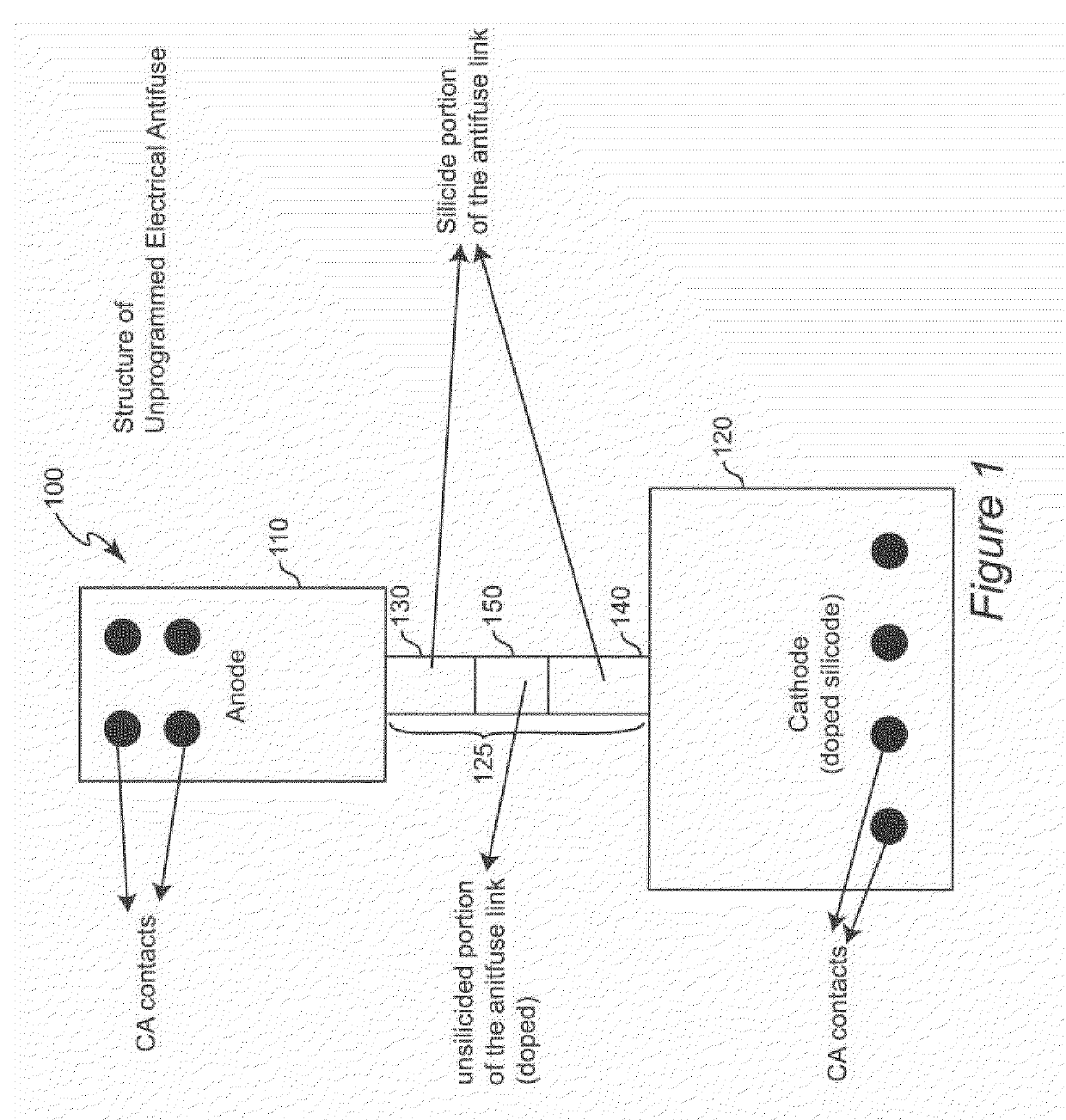
[0030]Referring now to the drawings, and more particularly to FIG. 1, there is shown, in plan view, a schematic representation of an antifuse in accordance with the present invention. Basically, the antifuse 100 in accordance with the present invention includes two enlarged rectangular terminal portions designated as an anode 110 and a cathode 120, each of which preferably comprises a stack of a polycrystalline silicon containing material layer and a silicide containing layer. The present invention can also be implemented in other technologies such as in a monocrystal line layer over a buried oxide (BOX) layer in semiconductor-on-insulator technology or other embodiments which will be apparent to those skilled in the art in view of the following discussion which, for clarity, will be provided in connection with the preferred polysilicon structure but which should be understood as inclusive of and comprehending other technologies and materials.

[0031]The preferred polycrystalline sili...


PUM

PropertyMeasurementUnit
voltagesaaaaaaaaaa
thicknessaaaaaaaaaa
thicknessaaaaaaaaaa

Abstract

An antifuse having a link including a region of unsilicided semiconductor material may be programmed at reduced voltage and current and with reduced generation of heat by electromigration of metal or silicide from a cathode into the region of unsilicided semiconductor material to form an alloy having reduced bulk resistance. The cathode and anode are preferably shaped to control regions from which and to which material is electrically migrated. After programming, additional electromigration of material can return the antifuse to a high resistance state. The process by which the antifuse is fabricated is completely compatible with fabrication of field effect transistors and the antifuse may be advantageously formed on isolation structures.

Description

BACKGROUND OF THE INVENTION[0001]1. Field of the Invention[0002]The present invention generally relates to electrical antifuses and, more particularly, to antifuses which are compatible with current CMOS manufacturing processes and which can be programmed easily, rapidly and with high reliability to alter electrical characteristics thereof by a readily detectable margin.[0003]2. Description of the Prior Art[0004]The use of fuses and antifuses in integrated circuits has become widespread in recent years, particularly for substituting spare circuits or circuit elements for defective circuits and circuit elements in order to increase manufacturing yield and avoid economic losses due to costs incurred in fabricating an integrated circuit which may not meet required specifications. Further, fuses and antifuses have been used to tailor circuit parameters for optimal performance and to electronically identify chips such as radio frequency (RF) chip identification. In recent years, fuses, i...

Claims


Application Information

Patent Timeline
Patent Type & Authority Applications(United States)
IPC IPC(8): H01L23/525H01L21/768
CPCH01L23/5252H01L2924/0002H01L2924/00H01L21/82H01L21/44H01L23/62
Inventor CESTERO, ALBERTOPARK, BYEONGJUSAFRAN, JOHN M.
Owner MARVELL ASIA PTE LTD
Why Eureka
Try Eureka