Semiconductor memory testing device and test method using the same

a test device and memory technology, applied in semiconductor/solid-state device testing/measurement, semiconductor/solid-state device details, instruments, etc., can solve the problems of affecting the efficiency of maintaining the affordability of external test devices with clock frequencies that can match the high-speed semiconductor memory devices, raising the bit-rate of data, and not being able to generate various test data used for performing the test of the semiconductor memory devices

Active Publication Date: 2009-04-07
SAMSUNG ELECTRONICS CO LTD
View PDF17 Cites 13 Cited by
  • Summary
  • Abstract
  • Description
  • Claims
  • Application Information

AI Technical Summary

Problems solved by technology

In particular, since there is a rapidly increasing trend for high-speed memory products that exceed 500 MHz in clock frequency, and because manufacturing costs for the external test device are high, it is difficult to efficiently maintain the affordability of external test devices that have a clock frequency that can match that of the high-speed semiconductor memory devices.
Although the clock doubling test mode may raise the operating frequency by multiplying the external clock signal CLK, the clock doubling test mode may not raise a bit-rate on a data input.
In the conventional method, although the clock frequency of the internal clock signal may be increased, it is not possible to generate various test data used for performing the test of the semiconductor memory device.
As a result, it is difficult to effectively utilize the advantage of a high-rate operating frequency of the internal clock signal.

Method used


Image

  • Semiconductor memory testing device and test method using the same
  • Semiconductor memory testing device and test method using the same
  • Semiconductor memory testing device and test method using the same

Examples


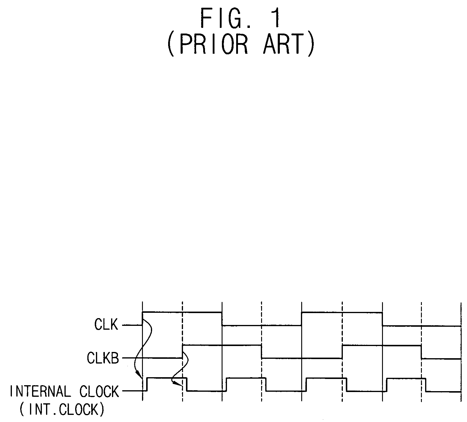
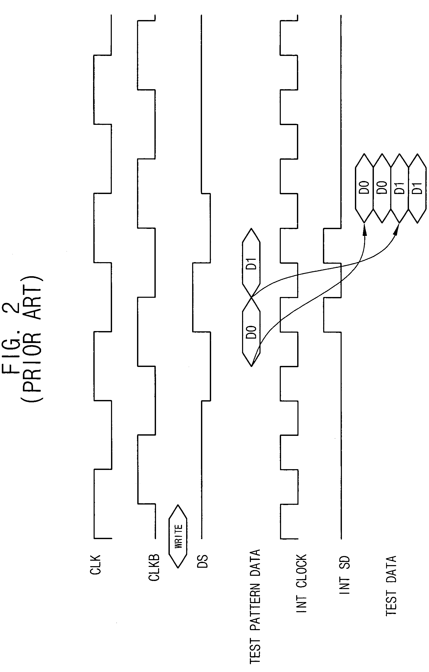
Embodiment Construction

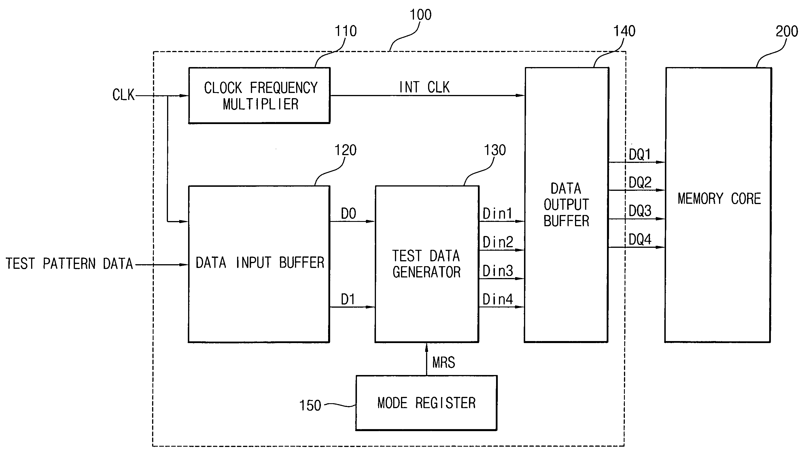
[0033]Detailed illustrative embodiments of the invention are disclosed below. Specific structural and functional details disclosed herein are merely representative for purposes of describing exemplary embodiments of the invention. The invention may, however, be embodied in many alternate forms and should not be construed as limited to the embodiments set forth herein.

[0034]Accordingly, while the invention is susceptible to various modifications and alternative forms, specific embodiments thereof are shown by way of example in the drawings and will herein be described in detail. It should be understood, however, that there is no intent to limit the invention to the particular forms disclosed, but on the contrary, the invention is to cover all modifications, equivalents, and alternatives falling within the spirit and scope of the invention. Like numbers refer to like elements throughout the description of the figures.

[0035]It will be understood that, although terms such as first, seco...


PUM


Abstract

A test device for a semiconductor memory device includes a clock frequency multiplier, a data input buffer, a test data generator and a data output buffer. The clock frequency multiplier multiplies an external clock signal having a relatively low frequency provided from an external test device to generate an internal clock signal having a relatively high frequency. The data input buffer buffers test pattern data provided in synchronization to the external clock signal to output the buffered test pattern data. The test data generator generates test data that is to be synchronized to the internal clock signal, using the outputted test pattern data based on a first or a second control signal. The data output buffer outputs the generated test data to a memory core of the semiconductor memory device. The test device generates various test data suitable for a memory test at a high operating speed.

Description

CROSS REFERENCE TO RELATED APPLICATIONS[0001]This application claims priority from Korean Patent Application No. 10-2005-0006297 filed on 24 Jan. 2005 in the Korean Intellectual Property Office. Korean Patent Application No. 10-2005-0006297 is incorporated by reference in its entirety.BACKGROUND[0002]1. Technical Field[0003]This disclosure relates to a semiconductor memory test device and a test method using the same, and more particularly to semiconductor memory test devices that are capable of performing a high-speed memory test using various test data, and test methods using the same.[0004]2. Description of the Related Art[0005]Generally, a memory device is used to temporarily or permanently storing data and / or commands for computers, communication systems, image processing systems and so on. Examples of the memory device include semiconductor memory devices, tapes, magnetic disks and optical disks. Currently, the semiconductor memory device is the predominant memory device.[0006...

Claims


Application Information

Patent Timeline
Patent Type & Authority Patents(United States)
IPC IPC(8): G01R31/28
CPCG11C29/12015G11C29/14G11C29/36G11C29/56004G11C29/56012G11C2029/3602G11C2029/5602G11C29/00G01R31/26H01L22/00
Inventor JEONG, TAE-JINSHIN, SANG-WOONG
Owner SAMSUNG ELECTRONICS CO LTD
Why Eureka
Try Eureka