Light emitting mesa structures with high aspect ratio and near-parabolic sidewalls

a technology of mesa structure and sidewall, which is applied in the direction of photovoltaic energy generation, electrical apparatus, semiconductor devices, etc., can solve the problems of not eliminating the requirement for an external mirror, and the inability to eliminate the long path length of the semiconductor chip, etc., to achieve the effect of reducing the d1/d2 ratio

Active Publication Date: 2009-04-14
META PLATFORMS TECH LLC
View PDF8 Cites 135 Cited by
  • Summary
  • Abstract
  • Description
  • Claims
  • Application Information

AI Technical Summary

Benefits of technology

[0031]In one embodiment, the device area covered with diode mesas is greater than 10 mm2, and wherein more than 80% of all extracted light is extracted through a back surface, whereby the device is scalable and suitable for high light outputs from a single array-chip.

Problems solved by technology

A major challenge is to extract as much of the emitted light as possible from the semiconductor material into the surrounding medium, usually air.
Long path lengths and reflections at metal coated semiconductor surfaces both lead to absorption losses.
However, it does not eliminate the long path lengths within the semiconductor chip, nor the requirement for an external mirror.
Also, the technique is less suitable to the widely used gallium nitride (GaN) based materials systems.
The reason for this is that the sapphire and silicon carbide (SiC) substrates commonly used in GaN-based LED-chips are both very hard materials and very difficult to shape mechanically, for example with a dicing saw.
In these materials systems it seems not to be a practical solution to shape the whole chip.

Method used


Image

  • Light emitting mesa structures with high aspect ratio and near-parabolic sidewalls
  • Light emitting mesa structures with high aspect ratio and near-parabolic sidewalls
  • Light emitting mesa structures with high aspect ratio and near-parabolic sidewalls

Examples


Embodiment Construction

Brief Description of the Drawings

[0044]The invention will be more clearly understood from the following description of some embodiments thereof, given by way of example only with reference to the accompanying drawings in which:—

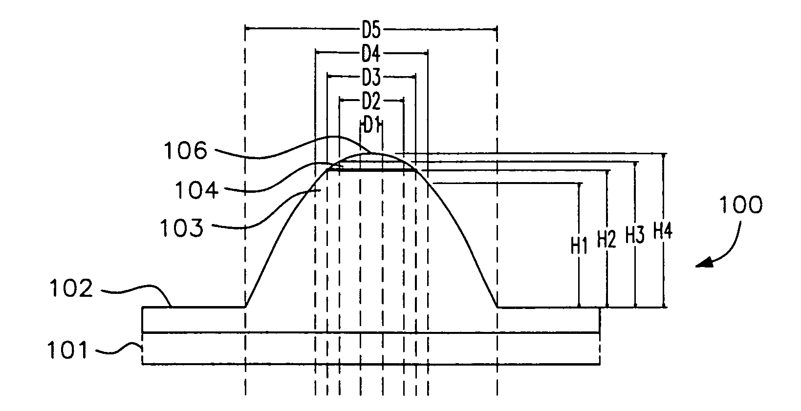
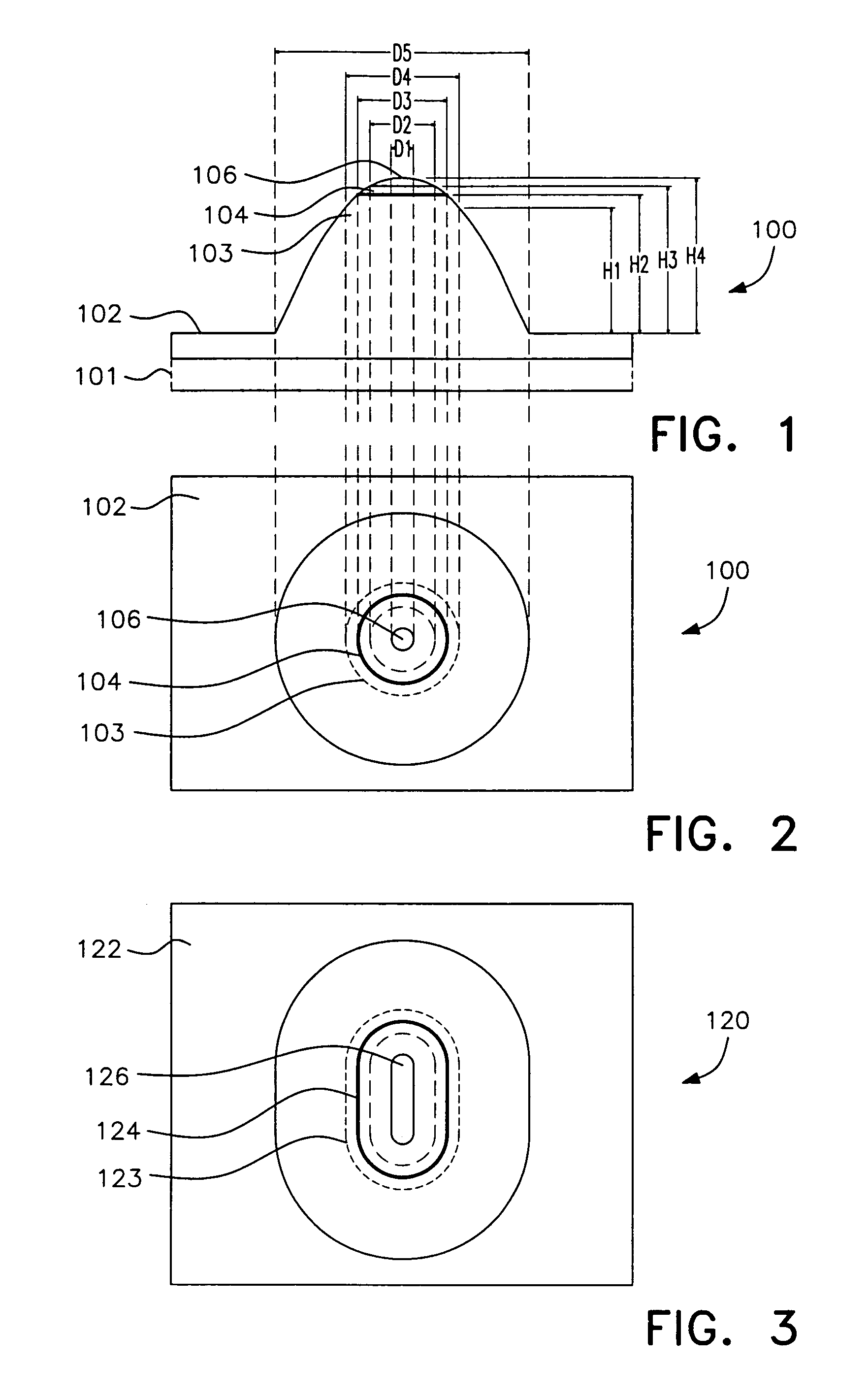
[0045]FIG. 1 is a diagrammatic cross sectional view of a single element of a micro LED array device, and

[0046]FIG. 2 is a plan view;

[0047]FIG. 3 is a plan view of an alternative device;

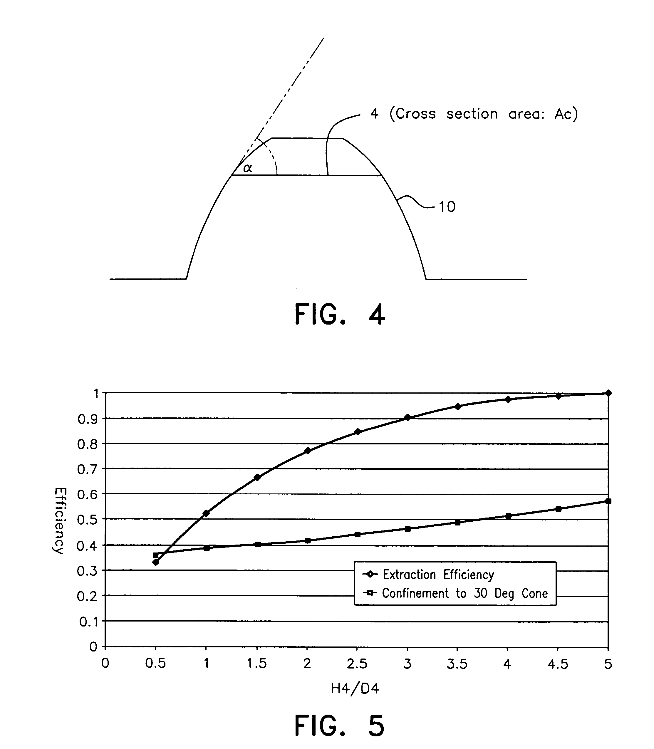
[0048]FIG. 4 defines the angle α between the light emitting layer (LEL) and the mesa sidewall;

[0049]FIG. 5 is a plot of extraction efficiency into air versus aspect ratio (H4 / D4) for paraboloid shaped reflectors in semiconductor material with a refractive index of 2.28;

[0050]FIG. 6 shows the effect of the top electrical contact reflectivity on the results obtained in FIG. 5;

[0051]FIG. 7 is a plot showing the effect of the light emitting layer position with respect to the focal plane of the paraboloid (the focal plane being defined as the horizontal plane that intersects the foc...


PUM


Abstract

An array of highly efficient micro-LEDs where each micro-LED is an integrated diode structure in a mesa, in which the mesa shape and the light-emitting region are chosen for optimum efficiency. A single one of the micro-LEDs includes, on a substrate and a semiconductor layer, a mesa, a light emitting layer, and an electrical contact. The micro-LEDs in this device have a very high EE because of their shape. Light is generated within the mesa, which is shaped to enhance the escape probability of the light. Very high EEs are achieved, particularly with a near parabolic mesa that has a high aspect ratio. The top of the mesa is truncated above the light-emitted layer (LEL), providing a flat surface for the electronic contact on the top of the semiconductor mesa. It has been found that the efficiency is high, provided the top contact has a good reflectivity value. Also, it has been found that efficiency is particularly high if the contact occupies an area of less than 16% of the truncated top mesa surface area. This feature also helps to achieve a more directional beam in the case of the device being an LED.

Description

[0001]This is a continuation of PCT / IE2004 / 000063 filed 4 May 2004 and published in English.INTRODUCTION[0002]1. Field of the Invention[0003]The invention relates to light emitting diodes (LEDs) and photodiodes (PDs).[0004]2. Prior Art Discussion[0005]LEDs convert electrical energy into optical energy, and PDs convert optical energy into electrical energy. We will describe the invention as it relates to LEDs, and it will be readily understood that the invention can also be applied to the reverse, PD, operation.[0006]In semiconductor LEDs, light is usually generated through recombination of electrons, originating from an n-type doped semiconductor layer, and holes originating from a p-type doped semiconductor layer. In some infra-red emitting semiconductor materials light can be generated by electron intersub-band transitions rather than electron hole transitions. We will call the area where the main light generation takes place the light-emitting layer (LEL).[0007]A major challenge ...

Claims


Application Information

Patent Timeline
Patent Type & Authority Patents(United States)
IPC IPC(8): H01L27/15H01L29/26H01L31/12H01L33/00H01L25/075H01L31/0352H01L33/08H01L33/20H01L33/24
CPCH01L31/035281H01L33/08H01L33/20H01L33/24Y02E10/50
Inventor MAASKANT, PLEUN PIETERO'CARROLL, EDMUND ANTHONYLAMBKIN, PAUL MARTINCORBETT, BRIAN
Owner META PLATFORMS TECH LLC
Why Eureka
Try Eureka