Semiconductor device and method for manufacturing the same

a technology of semiconductor devices and semiconductor layers, applied in the direction of semiconductor devices, basic electric elements, electrical equipment, etc., can solve the problems of difficult to form only films having a high relative permittivity, the original object of increasing the capacity cannot be achieved, etc., to achieve good fet quality, improve interfacial quality, and increase the relative permittivity of the buffer layer

Inactive Publication Date: 2009-04-21
OHMI +1
View PDF18 Cites 51 Cited by
  • Summary
  • Abstract
  • Description
  • Claims
  • Application Information

AI Technical Summary

Benefits of technology

[0007]The present invention was made in consideration of the above described problems. It is a general object of the present invention to provide a semiconductor device having good quality by keeping the relative permittivity of a High-K insulation film in a high state. Another object of the present invention is to provide a method for manufacturing a semiconductor device in which the relative permittivity of the High-K insulation film can be kept in a high state.
[0009]As for the above described gate insulation film, it is preferable to form the film according to a plasma CVD technology. Further, in a case where a silicon nitride film is provided as a barrier layer between the silicon substrate and the gate insulation film, it is less likely that the thickness of the film increases while the High-K material is being formed. Thus, a decrease of the capacity can be controlled. This is based on the fact that the thickness of the silicon nitride film is less likely to increase than the thickness of the oxide film. It should be noted that the above described silicon nitride layer can be formed according to a direct nitriding by plasma processing.
[0011]Furthermore, a more stable insulation film can be obtained by laminating the silicon nitride films and the gate insulation films alternately on the silicon substrate.
[0012]Further, interfacial quality can be improved and a good FET quality can be obtained by forming a buffer layer between the silicon substrate and the gate insulation film.
[0013]In addition, the relative permittivity of the buffer layer can be increased to substantially 9 by forming an Alumina (Al2O3) monocrystal film between the silicon substrate and the gate insulation film. Accordingly, the capacity can be further increased. It should be noted that the above described alumina monocrystal film can be formed according to the plasma CVD technology.

Problems solved by technology

Therefore, the original object of increasing the capacity cannot be achieved.
Thus, it is difficult to form only a film having a high relative permittivity.

Method used


Image

  • Semiconductor device and method for manufacturing the same
  • Semiconductor device and method for manufacturing the same
  • Semiconductor device and method for manufacturing the same

Examples


first embodiment

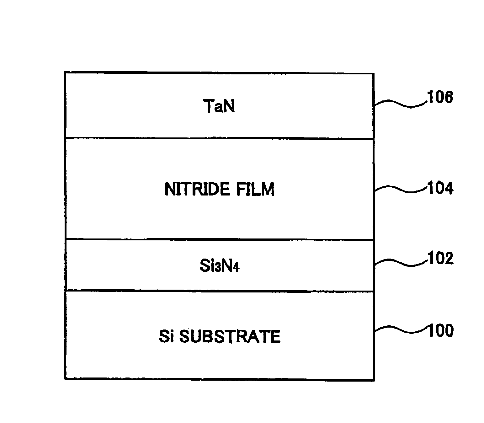
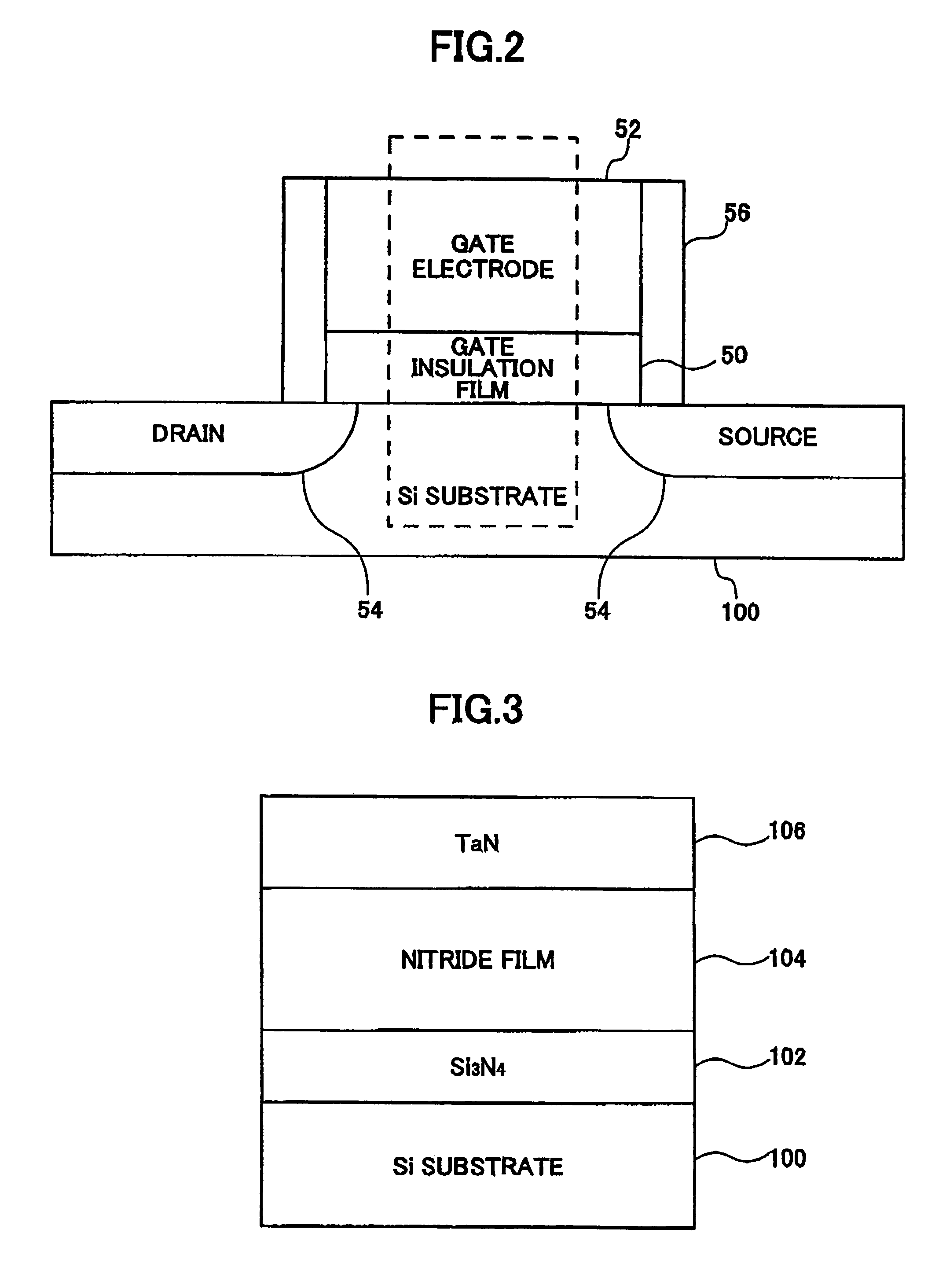
[0031]FIG. 3 is a schematic diagram showing the configuration of the substantial part of the semiconductor device according to the present invention. In the semiconductor device of the present embodiment, a nitride High-K film 104 is formed as a gate insulation film (50) on the silicon substrate 100. A silicon nitride film (Si3N4 layer) 102 is formed between the silicon substrate 100 and the High-K film 104. Further, a TaN layer 106 is formed as a gate electrode (52) on the High-K film 104 by spattering. The High-K film 104 is formed by using the plasma treatment device 10 according to a plasma CVD technology. The silicon nitride film 102 is formed in the same way by using the plasma treatment apparatus 10 according to a direct radical nitriding treatment. The silicon nitride film 102 performs a function of lowering the interface state.

[0032]As the High-K film 104, for example, one of the following compositions can be adopted:

[0033]

M3Si6N11(M = La, Ce, Pr, Nd, Sm);M2Si5N8(M = Ca, Sr...

third embodiment

[0038]FIG. 5 is a schematic diagram showing the configuration of the substantial part of the semiconductor device according to the present invention. In FIG. 5, the same or the corresponding components of FIG. 3 and FIG. 4 are allocated the same reference numbers, and overlapping descriptions are omitted. In the configuration of the present embodiment, the High-K film 104 is formed between the silicon substrate 100 and the gate electrode layer (TaN layer); however, another layer such as a Si3N4 layer is not formed between the silicon substrate 100 and the High-K film 104 or between the High-K film 104 and the TaN layer 106.

fourth embodiment

[0039]FIG. 6 is a schematic diagram showing the configuration of the substantial part of the semiconductor device according to the present invention. In FIG. 6, the same or the corresponding components of FIG. 3 through FIG. 5 are allocated the same reference numbers, and overlapping descriptions are omitted. In the configuration of the present embodiment, a buffer layer 110 is formed between the silicon substrate 100 and the High-K film 104. It should be noted, however, that another layer such as a Si3N4 layer is not provided between the High-K film 104 and the TaN layer 106.

[0040]The buffer layer 110 is formed by changing the composition of the gas which is supplied to the treatment container 11 in the same process of forming the High-K film 104. The buffer layer 110 has the benefit of a relative permittivity higher than that of the Si3N4 layer, and an interface state which can be lowered.


PUM


Abstract

In order to provide a semiconductor device having good quality by keeping the relative permittivity of a High-K insulation film in a high state, or to provide a method for manufacturing a semiconductor device in which the relative permittivity of the High-K insulation film can be kept in a high state, a semiconductor device is disclosed that includes a silicon substrate, a gate electrode layer, and a gate insulation film between the silicon substrate and the gate electrode layer. The gate insulation film is a high relative permittivity (high-k) film being formed by performing a nitriding treatment on a mixture of a metal and silicon. The High-K film itself becomes a nitride so as to prevent SiO2 from being formed.

Description

TECHNICAL FIELD[0001]The present invention generally relates to an improvement of a semiconductor device in which a high relative permittivity (high-k) film is used as a gate insulation film.BACKGROUND ART[0002]In the conventional technology, polysilicon (Poly-Si) is mainly used as an electrode material which is formed on a silicon substrate. As a gate insulation film provided between the silicon substrate and the polysilicon electrode material, a silicon oxide (SiO2), a silicon oxynitride (SiON), and a silicon nitride (Si3N4) are used. As a related matter, in order to increase the capacity (proportional to ∈ / d, where e is relative permittivity, and d is film thickness) of the gate insulation film, the thickness of the gate insulation film (SiO2 (∈=3.9)) is conventionally reduced.[0003]According to Japanese Laid-Open Patent Application No. 2000-294550, a method is disclosed wherein a gate insulation film having an equivalent oxide thickness of 1 nm or less is provided by performing ...

Claims


Application Information

Patent Timeline
Patent Type & Authority Patents(United States)
IPC IPC(8): H01L21/336H01L21/04H01L21/28H01L21/318H01L29/51H01L29/78
CPCH01L21/28167H01L21/318H01L29/513H01L29/518H01L21/28194H01L21/28202H01L21/0217H01L21/02107H01L21/02247H01L21/02252
Inventor OHMITERAMOTO, AKINOBUWAKAMATSU, HIDETOSHIKOBAYASHI, YASUO
Owner OHMI
Why Eureka
Try Eureka