Nonvolatile memory and electronic apparatus

a non-volatile memory and electronic device technology, applied in the direction of electrical devices, semiconductor devices, transistors, etc., can solve the problems of source-drain breakdown voltage, serious problems in the operation of non-volatile memory, data stored in the dram or the sram are lost,

Inactive Publication Date: 2009-05-19
SEMICON ENERGY LAB CO LTD
View PDF93 Cites 76 Cited by
  • Summary
  • Abstract
  • Description
  • Claims
  • Application Information

AI Technical Summary

Benefits of technology

[0014]The present invention has been made in view of the above problems, and an object of the invention is therefore to realize a high-performance memory by effectively preventing or weakening the short channel effect that occurs in miniaturizing nonvolatile memories.
[0020]According to a sixth aspect of the invention, there is provided a nonvolatile memory comprising a substrate having an insulating surface; a source region, a drain region, and an active region that are formed over the substrate by using a semiconductor thin film that is a single crystal or is substantially regarded as a single crystal; impurity regions provided locally in the active region by adding an impurity element that is a group-13 or group-15 element, the impurity regions serving to prevent a depletion layer from expanding from the drain region toward the source region; and an intrinsic or substantially intrinsic channel forming region interposed between the impurity regions.

Problems solved by technology

If the power is turned off, data stored in the DRAM or the SRAM are lost.
However, since basically nonvolatile memories store data according to the same principle of operation as field-effect transistors (hereinafter referred to as FETs), the short channel effect, which is known as causing serious problems in the FET operation, also causes serious problems in the operation of nonvolatile memories as the miniaturization advances.
In particular, the phenomenon called “punch-through” decreases the source-drain breakdown voltage and hence makes the current control with the gate electrode difficult.
However, in the SSW-DSA structure, a large amount of holes thus generated act in no other way than flow into the substrate terminal.
This may cause a problem that a parasitic source-substrate-drain bipolar is formed to cause a kink phenomenon (an abnormal increase in drain current).

Method used


Image

  • Nonvolatile memory and electronic apparatus
  • Nonvolatile memory and electronic apparatus
  • Nonvolatile memory and electronic apparatus

Examples


embodiment 1

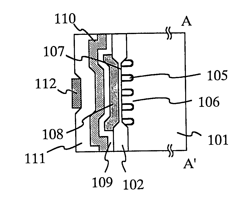
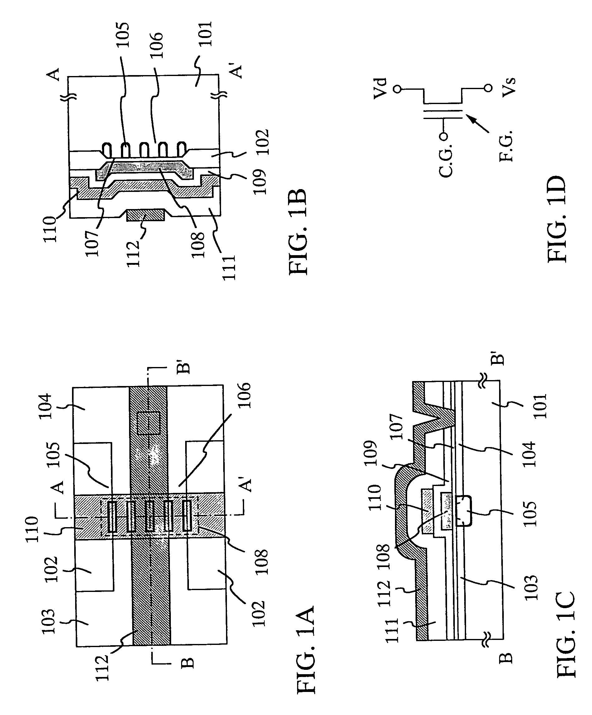
[0043]This embodiment will be described with reference to FIGS. 1A-1D, which are a top view, sectional views, and a circuit representation of a non-volatile memory to which the invention is applied. This embodiment is directed to an EEPROM having a basic stacked structure.

[0044]In FIGS. 1A-1D, reference numeral 101 denotes a single crystal silicon (p-type silicon) substrate; 102, field oxide films formed by a LOCOS method; 103, a source region to which arsenic (or phosphorus) is added; and 104, a drain region. Although this is an example structure of an n-type EEPROM, it is also possible to construct a p-type EEPROM. A p-type EEPROM can be constructed by forming source and drain regions by adding boron to an n-type silicon substrate.

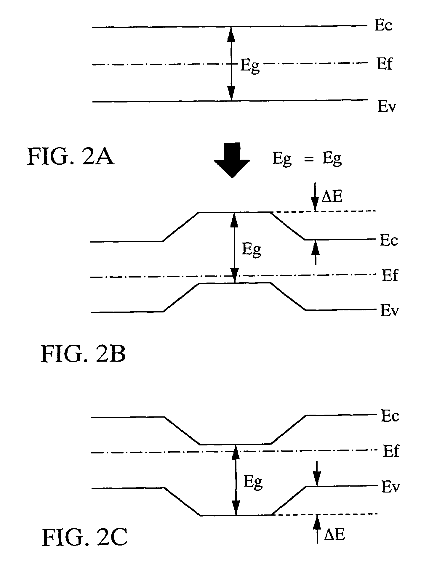
[0045]Reference numeral 105 denotes impurity regions (hereinafter referred to as pinning regions) that are the most important feature of the invention. The pinning regions 105 are formed by adding an impurity having the same conductivity type as the sili...

embodiment 2

[0108]This embodiment will be described with reference to FIGS. 6A-6D, which are a top view, sectional views, and a circuit representation of a non-volatile memory according to the invention that uses a single crystal silicon substrate having a buried oxide film. This embodiment is directed to an EEPROM having a basic stacked structure.

[0109]In FIGS. 6A-6D, reference numeral 600 denotes a single crystal silicon (p-type silicon) substrate; 601, a buried oxide film; 602, field oxide films formed by a LOCOS method; 603, a source region to which arsenic (or phosphorus) is added; and 604, a drain region.

[0110]Although this is an example structure of an n-type EEPROM, it is also possible to construct a p-type EEPROM. A p-type EEPROM can be constructed by forming source and drain regions by adding boron to an n-type silicon substrate.

[0111]The single crystal silicon substrate having a buried oxide film may be a SIMOX substrate, a UNIBOND substrate (a smart cut method is used), or the like....

embodiment 3

[0146]The two-layer polysilicon EEPROMs of the first and second embodiments are classified into a byte erasure type (data erasure is performed on a unit memory element basis) and a flash type (data of collective memory elements are erased en bloc).

[0147]The flash EEPROM is also called the flash memory. The invention can be applied to either of the two types of EEPROMs.

[0148]There are various data erasing methods such as a source erasure type, a source / gate erasure type, and a substrate erasure type. The invention can be applied to any of those methods.


PUM


Abstract

An active region, a source region, and a drain region are formed on a single crystal semiconductor substrate or a single crystal semiconductor thin film. Impurity regions called pinning regions are formed in striped form in the active region so as to reach both of the source region and the drain region. Regions interposed between the pinning regions serve as channel forming regions. A tunnel oxide film, a floating gate, a control gate, etc. are formed on the above structure. The impurity regions prevent a depletion layer from expanding from the source region toward the drain region.

Description

[0001]This application is a continuation of U.S. application Ser. No. 09 / 192,745, filed on Nov. 16, 1998 (now U.S. Pat. No. 6,686,623 issued Feb. 3, 2004).BACKGROUND OF THE INVENTION[0002]1. Field of the Invention[0003]The present invention relates to the configuration of a nonvolatile memory formed by using a semiconductor. In particular, the invention for a nonvolatile memory in which the channel length is 2 μm or less or even 0.5 μm or less.[0004]2. Description of the Related Art[0005]The IC memories that perform data storage and holding in computers are generally classified into the RAM and the ROM. Examples of the RAM (random access memory) are the DRAM (dynamic RAM) and the SRAM (static RAM). If the power is turned off, data stored in the DRAM or the SRAM are lost.[0006]On the other hand, examples of the ROM (read-only memory) are the mask ROM and the PROM (programmable ROM). The mask ROM and the PROM have an advantage that even if the power is turned off, data stored there ar...

Claims


Application Information

Patent Timeline
Patent Type & Authority Patents(United States)
IPC IPC(8): H01L29/788H01L21/28H01L21/336H01L27/115H01L27/12H01L29/423H01L29/786
CPCH01L21/28273H01L27/115H01L27/1203H01L29/42324H01L29/66825H01L29/78609H01L29/78675H01L29/7881H01L29/40114H10B69/00
Inventor YAMAZAKI, SHUNPEI
Owner SEMICON ENERGY LAB CO LTD
Why Eureka
Try Eureka