Organic light emitting diode display
a light-emitting diode and organic technology, applied in the field of organic light-emitting diodes, can solve the problems of low brightness, high power consumption, and difficulty in making large-sized lcd screens, and achieve the effect of emitted hea
- Summary
- Abstract
- Description
- Claims
- Application Information
AI Technical Summary
Benefits of technology
Problems solved by technology
Method used
Image
Examples
first embodiment
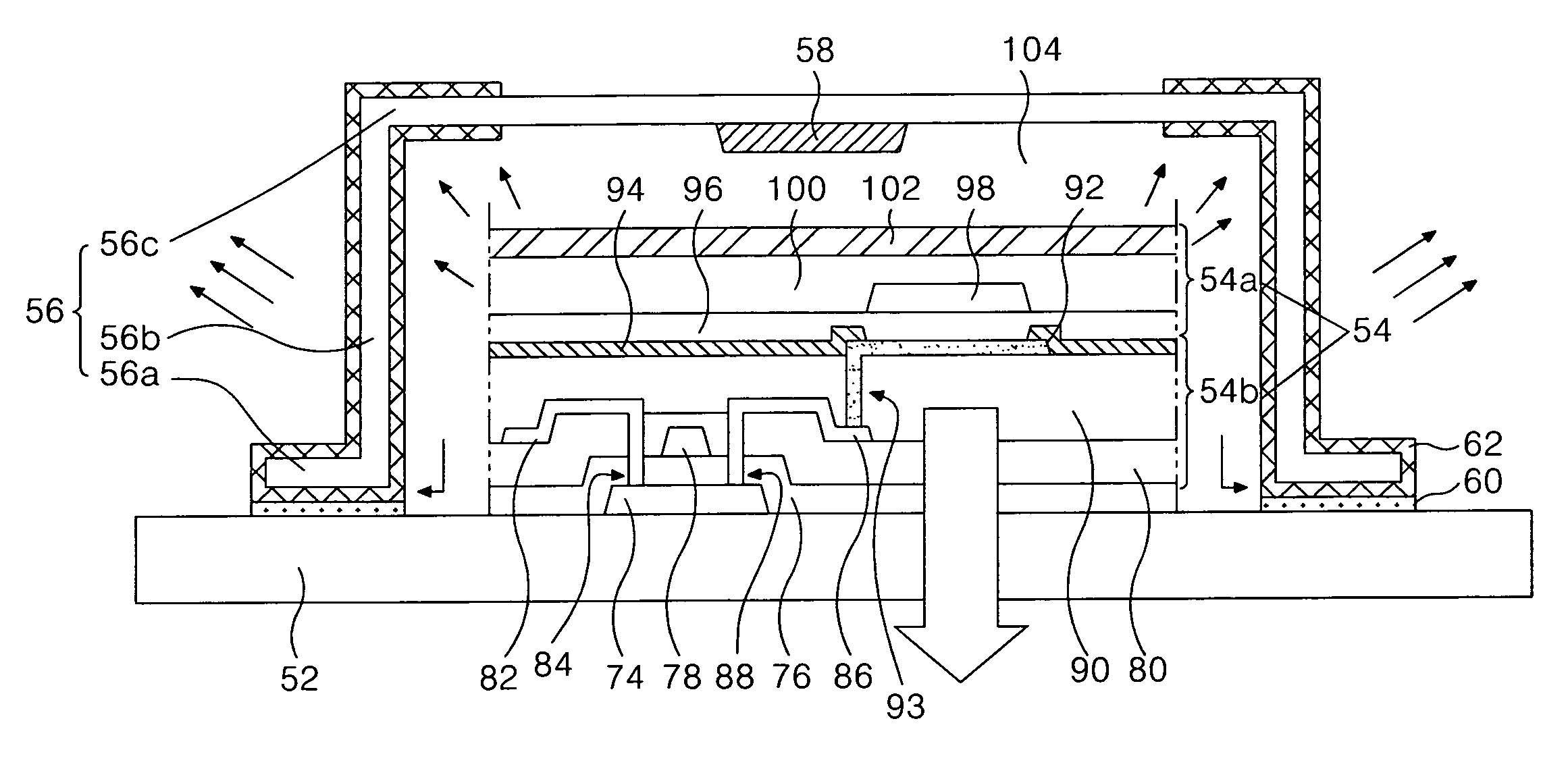
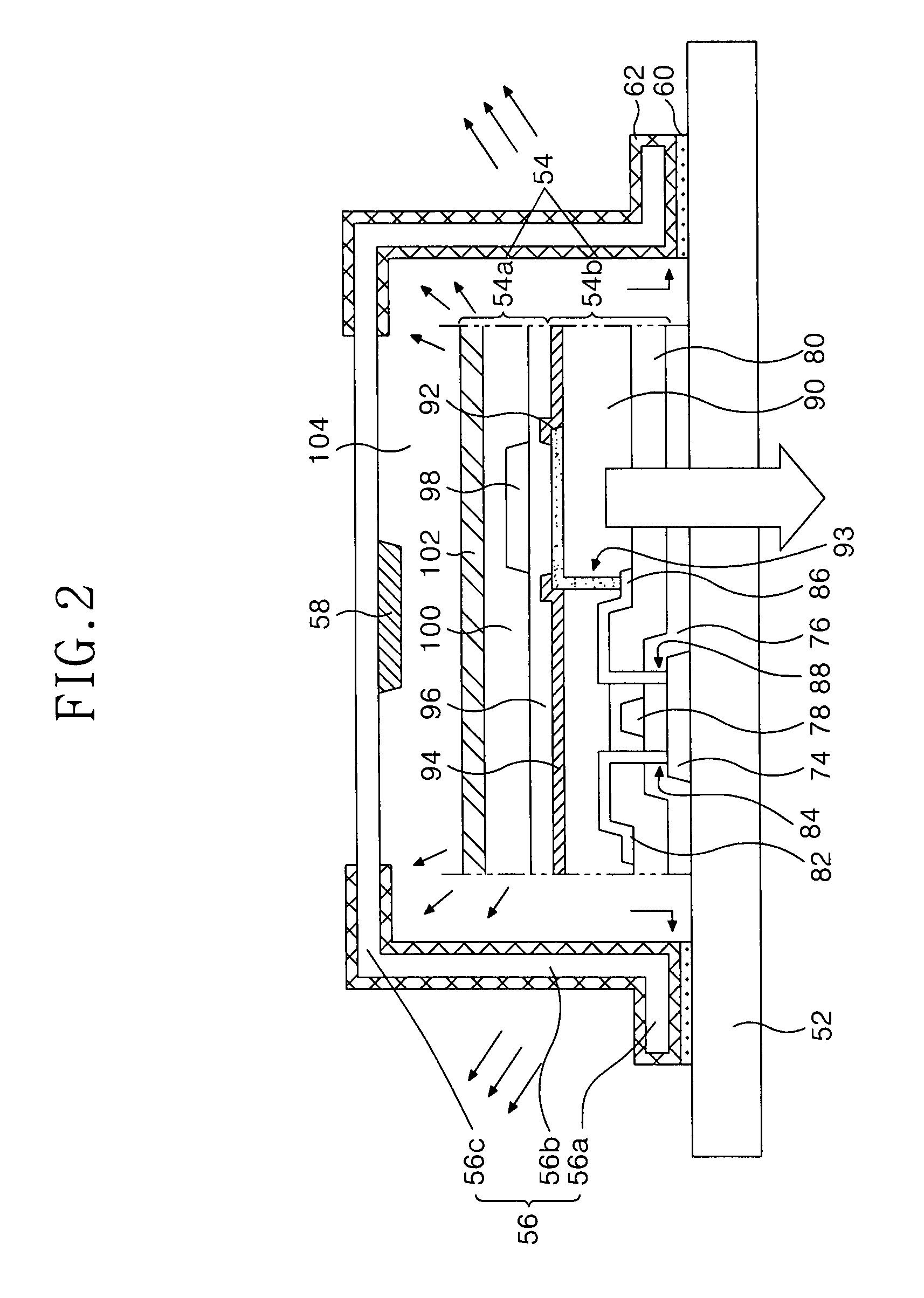
[0047]FIG. 3A, FIG. 3B, and FIG. 4 are diagrams showing the cap 56 on which the metal coating layer 62 is coated. In other words, FIG. 3A is a plan view which is shown when the observer observes the cap 56 at an outer surface of the upper flat surface part 56c which borders with an external air layer, and FIG. 3B and FIG. 4 are a plan view and a perspective view which are shown when the observer observes the cap 56 at an inner surface of the upper flat surface part 56c which borders with an internal air layer 104, respectively.
[0048]Referring to FIG. 3A, FIG. 3B, and FIG. 4, the metal coating layer 62 is formed at the bonding surface 56a of the cap 56, at an inner surface of the side wall 56b which borders with the internal air layer 104, at an outer surface of the side wall 56b which borders with an external air layer, at an inner surface edge of the upper flat surface part 56c which borders with the internal air layer 104, and at an outer surface edge of the upper flat surface par...
second embodiment
[0049]FIG. 5A and FIG. 5B are diagrams showing the cap 56 on which the metal coating layer 62 is coated. In other words, FIG. 5A and FIG. 5B are a plan view and a perspective view which are shown when the observer observes the cap 56 at an inner surface of the upper flat surface part 56c which borders with the internal air layer 104, respectively. Herein, a plan view which is shown when the observer observes the cap 56 at an outer surface of the upper flat surface part 56c which borders with an external air layer is the same as FIG. 3A.
[0050]Referring to FIG. 3A, FIG. 5A, and FIG. 5B, the metal coating layer 62 is formed at the bonding surface 56a of the cap 56, at an inner surface of the side wall 56b which borders with the internal air layer 104, at an outer surface of the side wall 56b which borders with an external air layer, at an inner surface edge of the upper flat surface part 56c which borders with the internal air layer 104, and at an outer surface edge of the upper flat s...
third embodiment
[0051]FIG. 6A and FIG. 6B are diagrams showing the cap 56 on which the metal coating layer 62 is coated. In other words, FIG. 6A and FIG. 6B are a plan view and a perspective view which are shown when the observer observes the cap 56 at an inner surface of the upper flat surface part 56c which borders with the internal air layer 104, respectively. Herein, a plan view which is shown when the observer observes the cap 56 at an outer surface of the upper flat surface part 56c which borders with an external air layer is the same as FIG. 3A.
[0052]Referring to FIG. 3A, FIG. 6A, and FIG. 6B, the metal coating layer 62 is formed at the bonding surface 56a of the cap 56, at an inner surface of the side wall 56b which borders with the internal air layer 104, at an outer surface of the side wall 56b which borders with an external air layer, at an inner surface edge of the upper flat surface part 56c which borders with the internal air layer 104, and at an outer surface edge of the upper flat s...
PUM
 Abstract
Description
Claims
Application Information


