Unlock instant, AI-driven research and patent intelligence for your innovation.

Flash memory device and programming and erasing methods therewith

a flash memory and programming technology, applied in the field of flash memory devices and programming and erasing methods there, can solve the problems of low erasing speed and inability to maintain the constant threshold voltage, and achieve the effect of ensuring the programming and erasing characteristics

Inactive Publication Date: 2009-05-26
DONGBU ELECTRONICS CO LTD
View PDF1 Cites 6 Cited by
  • Summary
  • Abstract
  • Description
  • Claims
  • Application Information

AI Technical Summary

Benefits of technology

This approach prevents the formation of trap sites, ensuring stable threshold voltage maintenance during programming and erasing, enhancing the efficiency and reliability of data storage by avoiding the issues associated with tunnel oxide layer damage and leakage currents.

Problems solved by technology

On erasing, in case of using an F-N (Fowler-Nordheim) tunneling instead of the hot hole injection method, it has the disadvantageous characteristics such as low erasing-speed.
As a result, it is impossible to maintain the constant threshold voltage due to the trap sites.

Method used


Image

  • Flash memory device and programming and erasing methods therewith
  • Flash memory device and programming and erasing methods therewith
  • Flash memory device and programming and erasing methods therewith

Examples


first embodiment

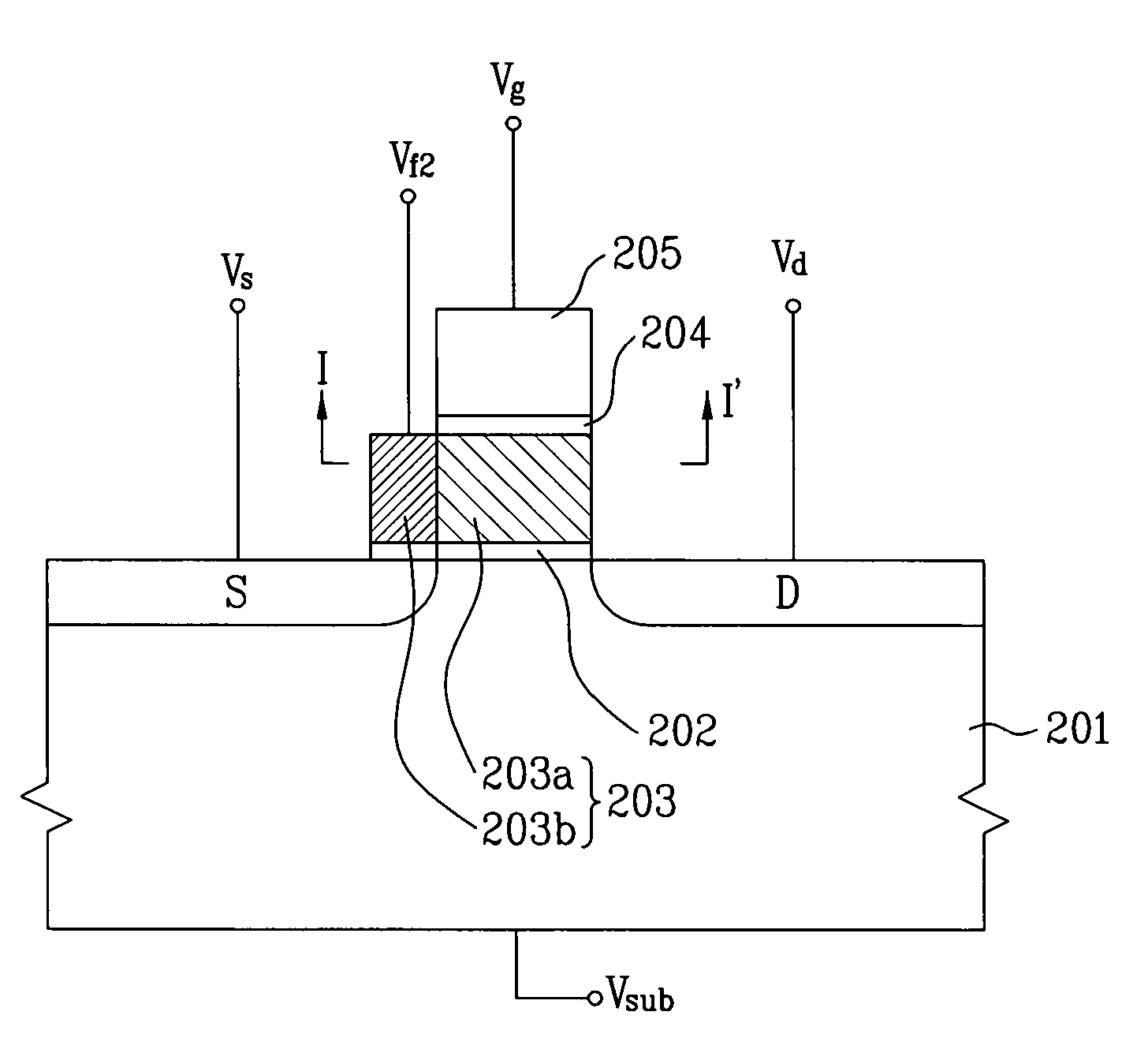
[0052]FIG. 2 shows a cross sectional view of a flash memory device according to the first embodiment of the present invention. In the flash memory device according to the first embodiment of the present invention, as shown in FIG. 2, a semiconductor substrate 201 is defined as a field area and an active area, and a device isolation layer (not shown) is formed in the field area.

[0053]In the active area of the semiconductor substrate 201, there are a tunnel oxide layer 202, a floating gate 203, a dielectric layer 204, and a control gate 205 formed in sequence. At this time, the semiconductor substrate 201 may be formed of n-type or p-type, wherein the p-type semiconductor substrate will be described for convenience of explanation. Although not shown, a passivation layer is deposited on an entire surface of the semiconductor substrate 201 including the control gate 205.

[0054]The dielectric layer 204 may be formed in a structure of oxide layer-nitride layer-oxide layer. Also, the floati...

second embodiment

[0067]A flash memory device according to the second embodiment of the present invention will be described as follows. FIG. 4 shows a cross sectional view of a flash memory device according to the second embodiment of the present invention.

[0068]In the flash memory device according to the second embodiment of the present invention, as shown in FIG. 4, a semiconductor substrate 201 is defined as a field area and an active area, and a device isolation layer (not shown) is formed in the field area. At this time, the semiconductor substrate 201 may be formed of n-type or p-type, wherein the p-type semiconductor substrate will be described for convenience of explanation.

[0069]In the active area of the semiconductor substrate 201, there are a tunnel oxide layer 202, a floating gate 203, a dielectric layer 204, and a control gate 205 formed in sequence. Then, n-type impurity ions are implanted into the semiconductor substrate 201 at both sides of the first floating gate 203 / the control gate...

third embodiment

[0085]A flash memory device according to the third embodiment of the present invention will be described with reference to FIG. 9. FIG. 9 shows a cross sectional view of a flash memory device according to the third embodiment of the present invention. In the flash memory device according to the third embodiment of the present invention, as shown in FIG. 9, a tunnel oxide layer 402, a floating gate 403, a dielectric layer 404 and a control gate 405 are sequentially deposited in an active area of a p-type semiconductor substrate 401 defined by a device isolation layer (not shown).

[0086]The floating gate 403 is comprised of a first floating gate 403a, a second floating gate 403b and a third floating gate 403c, wherein the first floating gate 403a is positioned in the center between the second floating gate 403b and the third floating gate 403c. At this time, the first floating gate 403a is formed at a width corresponding to that of the control gate 405.

[0087]Then, n-type impurity ions ...


PUM


Abstract

A flash memory device and programming and erasing methods therewith is disclosed, to secure the programming and erasing characteristics by changing a structure of a floating gate, in which the flash memory device includes a first conductive type semiconductor substrate defined as a field area and an active area; a tunnel oxide layer on the active area of the first conductive type semiconductor substrate; a floating gate on the tunnel oxide layer, having at least first and second floating gates having different levels of energy band gap; a dielectric layer on the floating gate; a control gate on the dielectric layer; and second conductive type source / drain regions in the active area of the first conductive type semiconductor substrate at both sides of the floating gate.

Description

CROSS-REFERENCE TO RELATED APPLICATIONS[0001]This application claims the benefit of Korean Application Nos. P2003-101389 and P2003-101387, filed on Dec. 31, 2003, which is hereby incorporated by reference as if fully set forth herein.BACKGROUND OF THE INVENTION[0002]1. Field of the Invention[0003]The present invention relates to a flash memory device and programming and erasing methods therewith, and more particularly, to a flash memory device and programming and erasing methods therewith, to secure the programming and erasing characteristics by changing a structure of a floating gate.[0004]2. Discussion of the Related Art[0005]Among semiconductor memory devices, a non-volatile memory device is an optimal device in that it is possible for a user to program data with easiness by switching a memory state in an electrical method, and also, it is possible to maintain the memory state of data even if a power is switched off.[0006]On the fabrication process, the non-volatile memory device...

Claims


Application Information

Patent Timeline
Patent Type & Authority Patents(United States)
IPC IPC(8): H01L29/94H01L21/8247G11C16/02G11C16/04G11C16/06G11C16/10H01L21/28H01L27/115H01L29/423H01L29/788H01L29/792
CPCG11C16/0425G11C16/10H01L21/28273H01L29/42324H01L29/40114
Inventor JUNG, JIN HYO
Owner DONGBU ELECTRONICS CO LTD