Method of fabricating substrate with embedded component therein

a technology of embedded components and substrates, which is applied in the direction of printed circuit manufacturing, printed circuit aspects, final product manufacturing, etc., can solve the problems that the requirements of light weight, thinness, shortness, and smallness of product design cannot be satisfied, and achieve the effect of reducing the thickness of the whole substrate and increasing the wiring density

Active Publication Date: 2009-06-23
ADVANCED SEMICON ENG INC
View PDF4 Cites 25 Cited by
  • Summary
  • Abstract
  • Description
  • Claims
  • Application Information

AI Technical Summary

Benefits of technology

[0012]Accordingly, the present invention is directed to providing a method of fabricating a substrate with an embedded component therein, so as to increase the wiring density of a first patterned circuit layer, a second patterned circuit layer, a first surface circuit, and a second surface circuit and significantly reduce the thickness of the whole substrate.
[0028]Based upon the above, regarding the method of fabricating the substrate with an embedded component therein provided by the present invention, the electrode of the embedded component is directly electrically connected to the first patterned circuit layer and the second patterned circuit layer in the inner layer, so as to enhance the wiring density of the first patterned circuit layer, the second patterned circuit layer, the first surface circuit, and the second surface circuit, and to improve the reliability of the electrical connection between the embedded component and the first patterned circuit layer or the second patterned circuit layer.
[0029]In addition, the embedded component is directly electrically connected to the patterned circuit layers in the inner layer without the conventional plated through hole (PTH), thereby efficiently reducing the thickness of the whole substrate such that the electronic products employing the substrate may satisfy the requirements of light weight, thinness, shortness, and smallness on product design.

Problems solved by technology

Additionally, the embedded component E must be electrically connected to the first surface circuit 122′ and the second surface circuit 132′ through the conductive vias V, which, however, increases the thickness of the whole circuit substrate and thus the requirements of light weight, thinness, shortness, and smallness on product design cannot be satisfied.

Method used


Image

  • Method of fabricating substrate with embedded component therein
  • Method of fabricating substrate with embedded component therein
  • Method of fabricating substrate with embedded component therein

Examples


Embodiment Construction

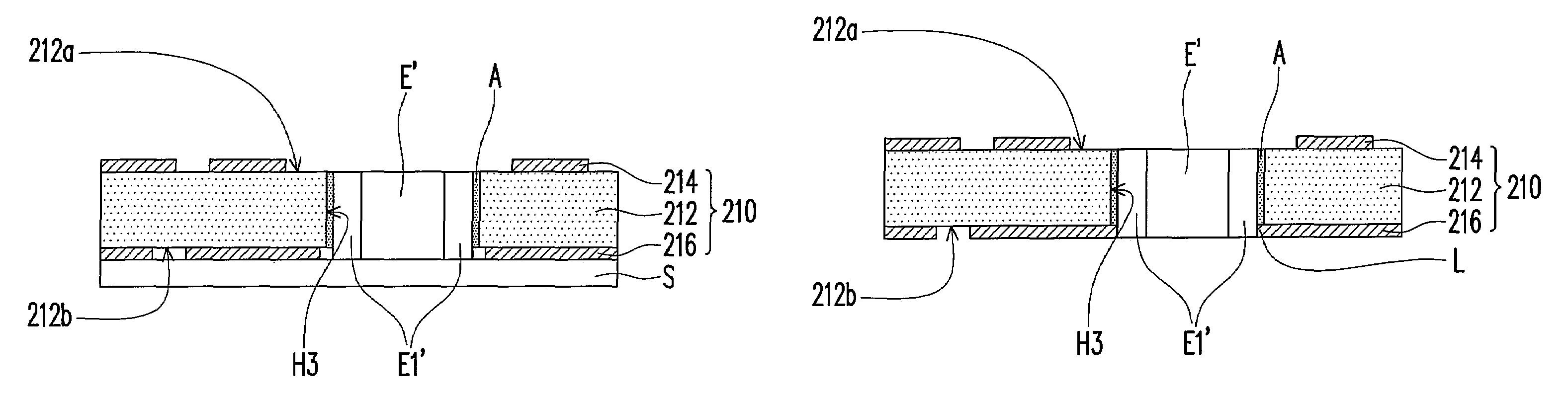
[0036]FIGS. 2A-2J are schematic sectional views of a fabricating flow of a substrate with an embedded component therein according to an embodiment of the present invention. Firstly, referring to FIG. 2A, a core layer 210 including a first dielectric layer 212, a first patterned circuit layer 214, and a second patterned circuit layer 216 is provided. The first patterned circuit layer 214 and the second patterned circuit layer 216 are disposed on an upper surface 212a and a lower surface 212b of the first dielectric layer 212, respectively. In this embodiment, the step of providing the core layer 210 includes patterning a first metal layer (not shown, and the material thereof is copper) and a second metal layer (not shown, and the material thereof is copper) on the upper surface 212a and the lower surface 212b of the first dielectric layer 212 through a lithography and etching process, respectively, so as to form the first patterned circuit layer 214 and the second patterned circuit l...


PUM

PropertyMeasurementUnit
electricallyaaaaaaaaaa
conductiveaaaaaaaaaa
dielectricaaaaaaaaaa

Abstract

A method of fabricating a substrate with an embedded component therein including the following steps is provided. First, a core layer having a first dielectric layer, a first patterned circuit layer, and a second patterned circuit layer is provided. The first patterned circuit layer and the second patterned circuit layer are disposed on an upper surface and a lower surface of the first dielectric layer, respectively. Then, a through hole is formed in the core layer. Next, the core layer is arranged on a supporting board and an embedded component having at least one electrode is disposed in the through hole. Afterward, a process of filling glue is carried out, such that the embedded component is fixed in the through hole. Thereafter, the supporting board is removed. Finally, the electrode of the embedded component is electrically connected to the second patterned circuit layer.

Description

CROSS-REFERENCE TO RELATED APPLICATION[0001]This application claims the priority benefit of Taiwan application serial no. 95104698, filed on Feb. 13, 2006. All disclosure of the Taiwan application is incorporated herein by reference.BACKGROUND OF THE INVENTION[0002]1. Field of Invention[0003]The present invention relates to a method of fabricating a substrate. More particularly, the present invention relates to a method of fabricating a substrate with an embedded component therein.[0004]2. Description of Related Art[0005]Generally speaking, a circuit substrate is mainly formed through alternately stacking a plurality of patterned circuit layers and dielectric layers, wherein the patterned circuit layers are defined and formed through a lithography and etching process on copper foils, and the dielectric layers are arranged between the patterned circuit layers for isolating two adjacent patterned circuit layers. Additionally, the adjacent patterned circuit layers are electrically conn...

Claims


Application Information

Patent Timeline
Patent Type & Authority Patents(United States)
IPC IPC(8): H01L21/50H01L21/44H01L21/48
CPCH05K1/186H05K3/4602H05K3/4652H05K2201/10636Y02P70/50
Inventor WANG, CHIEN-HAO
Owner ADVANCED SEMICON ENG INC
Why Eureka
Try Eureka