
Compound semiconductor epitaxial substrate

a technology of semiconductor epitaxial substrate and compound semiconductor, which is applied in the manufacture of semiconductor/solid-state devices, semiconductor devices, electrical apparatus, etc., can solve the problems of fluctuation of electrical characteristics of hbt, and achieve the effects of improving current gain characteristics of hbt, enhancing hbt characteristics, and propagating defects

Active Publication Date: 2009-06-23
SUMITOMO CHEM CO LTD +1
View PDF5 Cites 0 Cited by
  • Summary
  • Abstract
  • Description
  • Claims
  • Application Information

AI Technical Summary

Benefits of technology

[0010]In order to solve the above-described problems, in the present invention, in a compound semiconductor epitaxial substrate wherein a buffer layer, a sub-collector layer, a collector layer, a base layer and an emitter layer are formed on a substrate, an oxygen-containing layer is formed between the substrate and the sub-collector layer, and the propagation of defects existing in the substrate is suppressed by the oxygen-containing layer. Thereby, the fluctuation of the current gain characteristics of the HBT can be improved, and the HBT characteristics can be enhanced. In addition, a compound semiconductor epitaxial substrate that can obtain stable device characteristics not depending on the kinds of the substrate can be provided.

Problems solved by technology

Therefore, the current gain β of the HBT functional layers formed on the substrate is affected by the dislocation density of the substrate, there is a problem in that the fluctuation of electrical characteristics of the HBT is caused by the kind of the substrate to be used even if the same manufacturing process is applied.
However, by the constitution wherein the above-described lattice structure or super-lattice structure is formed in the buffer layer, the current gain characteristics still fluctuate depending on the kind of the substrate to be used, probably because the propagation of defects in the substrate into the epitaxial layer formed thereon cannot be sufficiently suppressed.

Method used


Image

  • Compound semiconductor epitaxial substrate
  • Compound semiconductor epitaxial substrate
  • Compound semiconductor epitaxial substrate

Examples


example 1

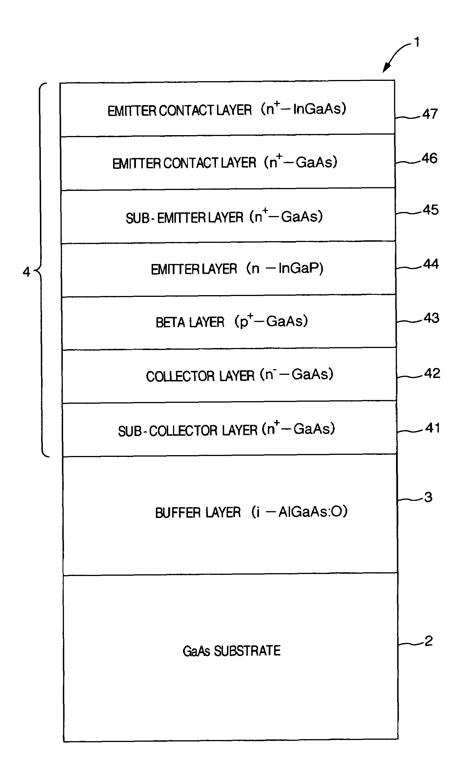
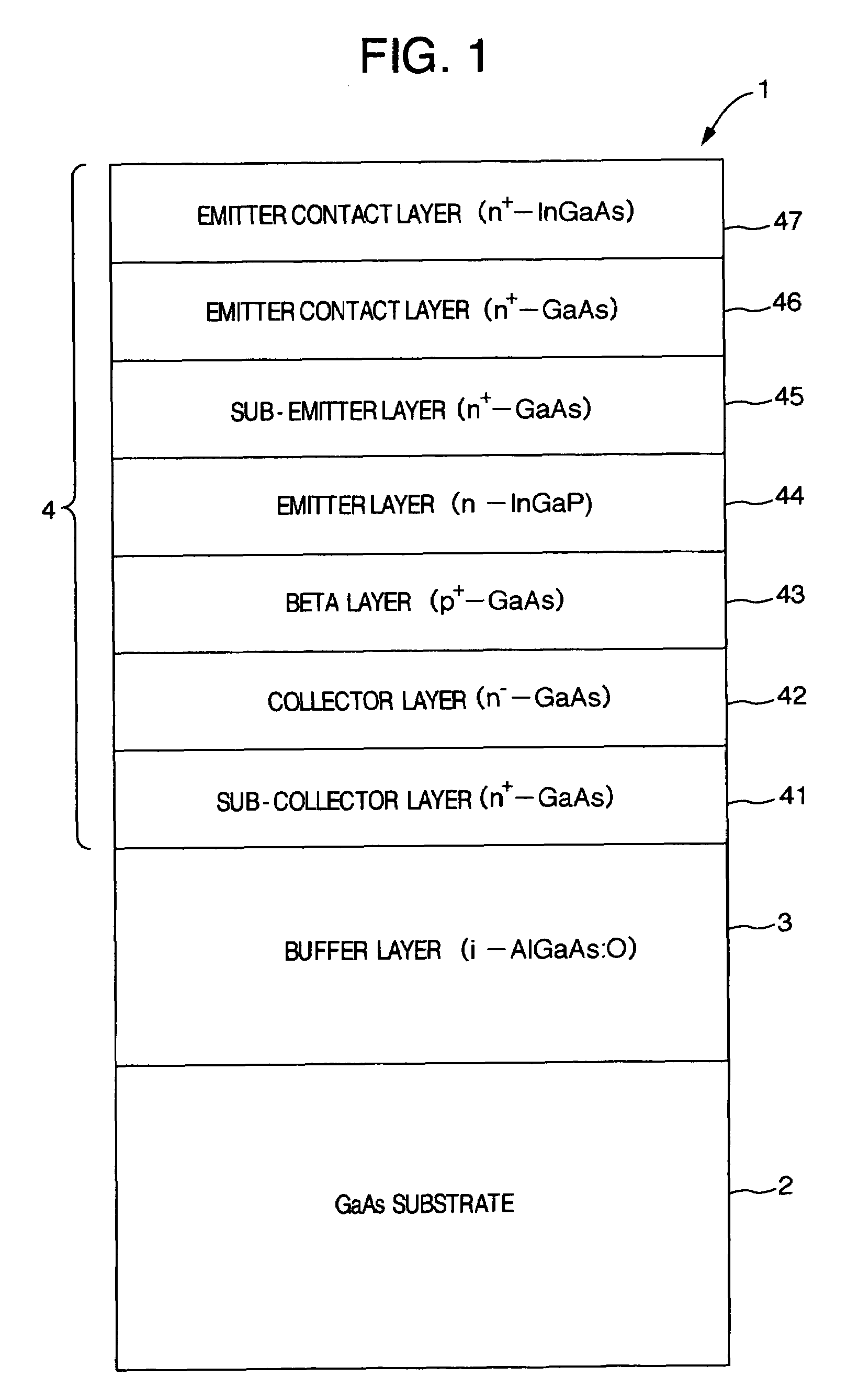
[0038]A compound semiconductor epitaxial substrate having a structure shown in FIG. 1 was fabricated as follows: A GaAs substrate having a defect density of 5000 / cm2 was prepared, and a buffer layer of Al0.3Ga0.7As of a thickness of 30 nm was grown on the GaAs substrate. At this time, ether was used as an oxygen supply source, and the oxygen concentration of the buffer layer was 1×1019 cm−3. HBT functional layers were formed on the buffer layer using an MOCVD process.

[0039]The thickness, in composition and the like were as follows: The emitter contact layer 47 was composed of an n+-InGaAs layer, the In composition was 0.5, the film thickness was 50 nm, and the carrier concentration was 2.0×1019 cm−3. The emitter contact layer 46 was composed of an n+-InGaAs layer, and the In composition was continuously varied from 0 at the boundary with the sub-emitter layer 45 to 0.5 at the boundary with the emitter contact layer 47, the film thickness was 50 nm, and the carrier concentration was ...

example 2

[0041]An HBT element was fabricated in the same manner as in Example 1, except that the defect density of the GaAs substrate used was 3000 to 4000 / cm2. The current gain β was measure to be 141.

example 3

[0042]An HBT element was fabricated in the same manner as in Example 1, except that the defect density of the GaAs substrate used was 3000 to 4000 / cm2, and the formation of a naturally occurring oxide film was suppressed. The current gain β was measure to be 141.


PUM


Abstract

A compound semiconductor epitaxial substrate including a substrate, and a sub-collector layer, a collector layer, a base layer, an emitter layer and a contact layer(s) formed in this order on the substrate, the compound semiconductor epitaxial substrate having an oxygen-containing layer between the substrate and the sub-collector layer.

Description

TECHNICAL FIELD[0001]The present invention relates to a compound semiconductor epitaxial substrate, and more specifically, relates to a compound semiconductor epitaxial substrate suitable for manufacturing a hetero-junction bipolar transistor.BACKGROUND ART[0002]A hetero-junction bipolar transistor (hereafter referred to as HBT in some cases) is a bipolar transistor wherein the emitter-base junction is made a hetero-junction using a substance having a larger band gap than the base layer for the emitter layer in order to enhance the emitter injection efficiency, and is suitable as a semiconductor element used in the frequency region of the microwave band or higher.[0003]For example, in the case of a GaAs HBT, a compound semiconductor epitaxial substrate wherein a p-n junction, which is an emitter-base junction, is the structure of the hetero-junction, is generally produced by sequentially crystal-growing an n+-GaAs layer (sub-collector layer), an n-GaAs layer (collector layer), a p-G...

Claims


Application Information

Patent Timeline
Patent Type & Authority Patents(United States)
IPC IPC(8): H01L29/739H01L31/072H01L21/205H01L21/331H01L29/08H01L29/205H01L29/207H01L29/737
CPCH01L29/0821H01L29/207H01L29/66318H01L29/7371H01L21/18
Inventor YAMADA, HISASHIOSADA, TAKENORIFUKUHARA, NOBORU
Owner SUMITOMO CHEM CO LTD
Learn More