Semiconductor chip and production thereof, and semiconductor device having semiconductor chip bonded to solid device
- Summary
- Abstract
- Description
- Claims
- Application Information
AI Technical Summary
Benefits of technology
Problems solved by technology
Method used
Image
Examples
first embodiment
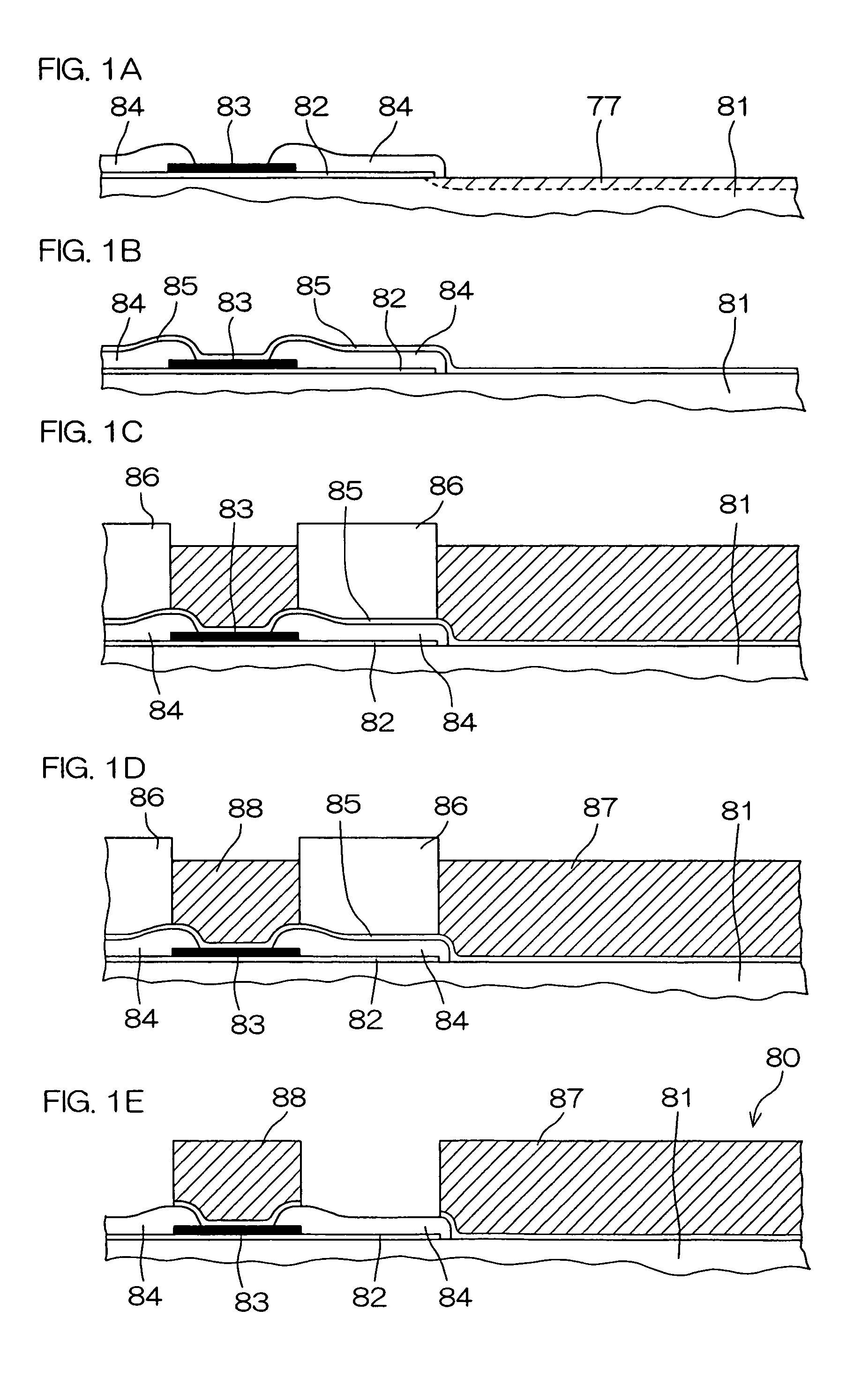
[0085]FIGS. 1A to 1E are sectional views of major portions for explaining the steps of a process for forming bumps of a semiconductor device in accordance with the present invention. In FIGS. 1A to 1E, a device formation region and a peripheral region surrounding the device formation region are illustrated. The following explanation is directed to an Si-based semiconductor device, but the semiconductor device may be based on any of various semiconductors such as a Ge semiconductor, and GaAs and GaP compound semiconductors.
[0086]As shown in FIG. 1A, an Al electrode 83 (an exposed portion of an internal interconnection) is formed in a predetermined position on an Si-based semiconductor substrate 81 with the intervention of a silicon oxide film 82. A peripheral portion of the Al electrode 83 is covered with a passivation film 84 such as of SiN or PSG. An impurity 77 of a predetermined conductivity type has been implanted at a high concentration in a peripheral region (e.g., a scribe li...
second embodiment
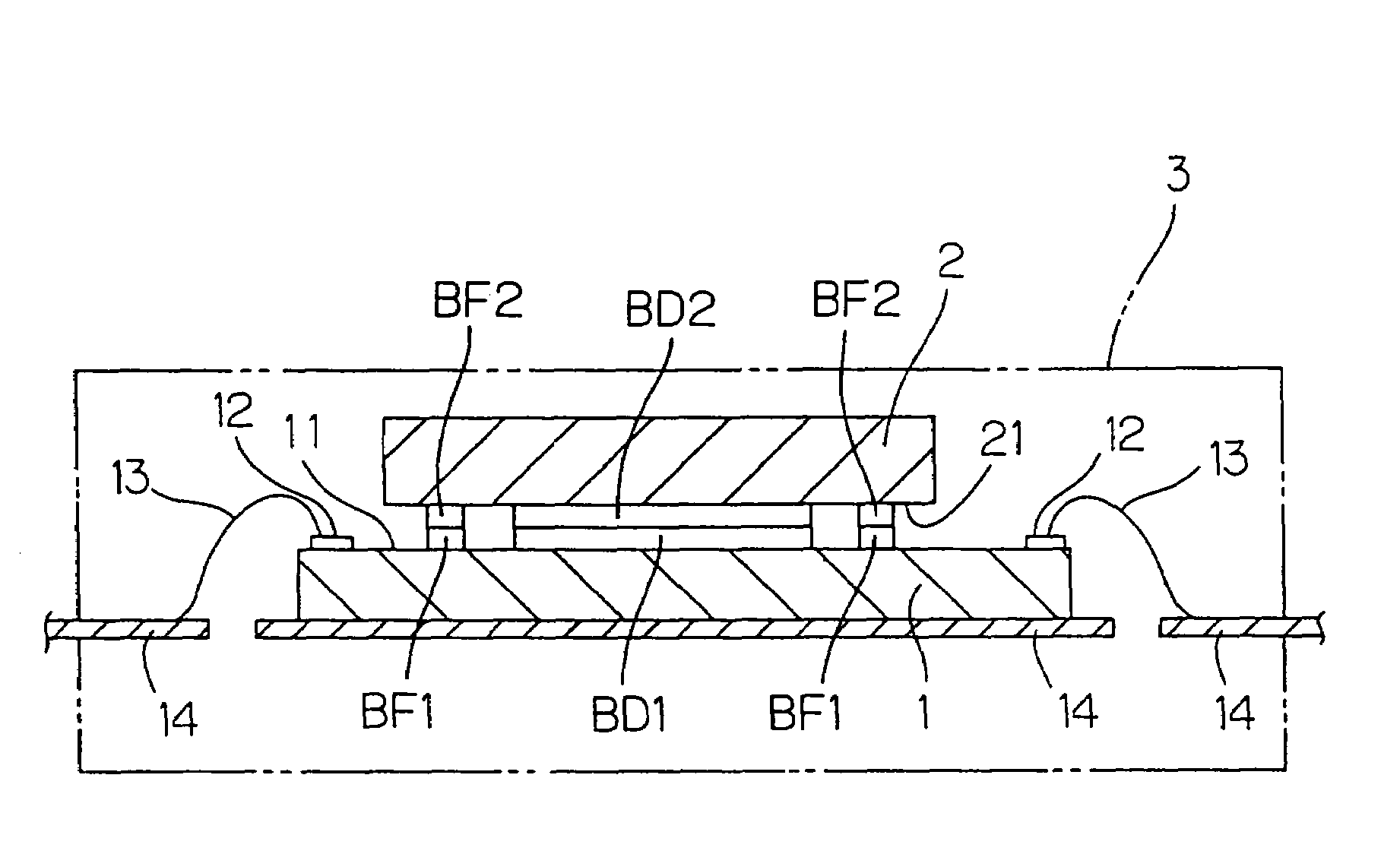
[0099]FIG. 5 is a schematic sectional view illustrating the construction of a semiconductor device which employs a semiconductor chip according to the invention. The semiconductor device has a so-called chip-on-chip structure, and is produced by bonding a secondary chip 2 onto a front face 11 of a primary chip 1 in a stacked relation and packaging the stacked semiconductor chips in a resin-sealed package 3.
[0100]The primacy chip 1 and the secondary chip 2 are, for example, silicon chips. The front face 11 of the primary chip 1 is a surface of a semiconductor substrate, which serves as a base of the primary chip 1, on the side of an active surface region formed with a functional device such as a transistor. A plurality of pads 12 for external connection are provided in a peripheral region of the front face 11, and connected to a lead frame 14 via bonding wires 13. A plurality of functional bumps BF1 for electrical connection to the secondary chip 2 and a dummy bump BD1 isolated from ...
third embodiment
[0111]FIG. 10 is a schematic sectional view illustrating the construction of a semiconductor device according to the invention. In FIG. 10, portions corresponding to those illustrated in FIG. 5 are denoted by the same reference characters as in FIG. 5. However, it is not intended that the portions denoted by the same reference characters in FIGS. 5 and 10 have identical constructions and functions.
[0112]The semiconductor device also has a chip-on-chip structure. That is, a secondary chip 2 is bonded to a primary chip 1 with a front face 21 thereof opposed to a front face 11 of the primary chip 11 by a so-called face-down method, and supported by a plurality of bumps provided therebetween. More specifically, a plurality of secondary bumps B2 are provided on the front face 21 of the secondary chip 2 as projecting therefrom, and a plurality of primary bumps B1 are provided on the front face 11 of the primary chip 1 in association with the secondary bumps B2 as projecting therefrom. The...
PUM
 Abstract
Description
Claims
Application Information


